|
FPGA DDR读写时序分析
使用Vivado中带的DDR的IP核可以方便进行DDR的读写,用户直接操控用户逻辑接口的信号,使信号满足时序逻辑即可。
具体时序逻辑请参照官方文档ug586_7Series_MIS.Pdf 下载链接: https://china.xilinx.com/support/documentation/ip_documentation/mig_7series/v4_2/ug586_7Series_MIS.pdf
借鉴文章链接: 基于Xilinx MIS IP的DDR3读写User Interface解析 https://wenku.baidu.com/view/63e8c92d195f312b3069a5ea.html
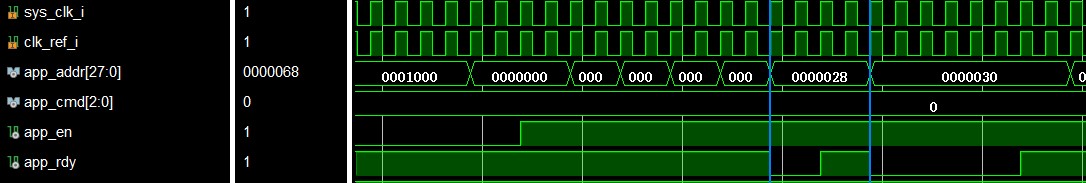
命令路径:
官方文档时序: app_rdy有效,从机已经处于等待接收状态,此时app_en有效,app_cmd和app_addr有效,则发送当前app_cmd中命令给DDR 控制IP。如果app_en有效,app_cmd和app_addr都有效,但是app_rdy处于忙状态,那么上面三个信号要保持有效状态,直到app_rdy处于空闲,即有效状态,才将命令发送给DDR控制IP。
 DDR示例工程仿真: 查看DDR IP的仿真,在第一个蓝色标志处上升沿,app_en有效,但是app_rdy处于忙状态,所以app_en保持高状态,app_cmd和app_addr保持有效状态,直到第一个蓝色标志处起第三个时钟上升沿app_rdy空闲,开始将app_cmd中指令发送给DDR IP控制器。第二个蓝色标志处也是一样,在蓝色标志处起第七个时钟,app_rdy空闲,发送app_cmd指令给DDR IP控制器。 DDR示例工程仿真: 查看DDR IP的仿真,在第一个蓝色标志处上升沿,app_en有效,但是app_rdy处于忙状态,所以app_en保持高状态,app_cmd和app_addr保持有效状态,直到第一个蓝色标志处起第三个时钟上升沿app_rdy空闲,开始将app_cmd中指令发送给DDR IP控制器。第二个蓝色标志处也是一样,在蓝色标志处起第七个时钟,app_rdy空闲,发送app_cmd指令给DDR IP控制器。
写入操作:
官方文档时序: 当app_rdy和app_wdf_rdy为高时,app_en为高,则开始发送数据到write fifo中。 DDR示例工程仿真: DDR示例工程仿真:
在写入时,app_rdy和app_wdf_rdy两个信号要处于有效状态。写入过程要写入128bit数据,共8个16bit数据,写入前6个数据时,app_wdf_rdy和app_rdy处于有效状态,在蓝色标注范围内,写第7个数据时,app_rdy为忙状态,所以第7和8两个数据并没有正常写入。
输入的命令和数据都有自己的FIFO用于存储,并且他们之间是同步的。数据比读写命令早或者晚写入都是可以的,因为他们在不同FIFO的同一层,同步时钟保证读写命令可以对应他需要操作的数据。如下所示,数据FIFO中只有一个3,对应着命令FIFO中的读,也就是会从FIFO中读个3出来,此时命令FIFO之后的写命令已经存进去了,但是数据FIFO与这些命令对应的操作数还没有写进去,但是即便是命令先写进去,数据后写进去也会写在响应命令对应的位置。数据比命令先写也是一样。
App_wdf_end信号,DDR3实际读写的Burst = 8。举例来说,DDR3的数据为宽为16bit,Burst为8,就是说每次对DDR3进行读写操作,必须是连续的8*16bit位数据。那么用户接口端,如果逻辑时钟为DDR3时钟的4分频,且数据位宽为128bit,那么单个时钟周期就应该对应Burst=8的一次读写操作;如果位宽为64bit,那么必须执行2次数据操作才能完成一次Burst=8的读写。对于前者app_wdf_end始终为1即可,对于后者app_wdf_end每2个写时钟周期内前一次拉低,后一次拉高。
App_wdf_data,app_wdf_wren和app_wdf_rdy,工作原理与命令路径类似。App_wdf_data有效,且app_wdf_wren拉高,必须app_wdf_rdy也为高,才表示当前数据写入DDR3 Controller IP。
读取操作:
官方文档时序: 当app_rd_data_vaild拉高时代表此时的app_rd_data有效。 当app_rd_data_vaild拉高时代表此时的app_rd_data有效。
示例工程仿真:
 下面贴上米联DDR3读写顶层代码方便对照学习 下面贴上米联DDR3读写顶层代码方便对照学习
//*****************************************************************************
// (c) Copyright 2009 - 2013 Xilinx, Inc. All rights reserved.
//
// This file contains confidential and proprietary information
// of Xilinx, Inc. and is protected under U.S. and
// international copyright and other intellectual property
// laws.
//
// DISCLAIMER
// This disclaimer is not a license and does not grant any
// rights to the materials distributed herewith. Except as
// otherwise provided in a valid license issued to you by
// Xilinx, and to the maximum extent permitted by applicable
// law: (1) THESE MATERIALS ARE MADE AVAILABLE "AS IS" AND
// WITH ALL FAULTS, AND XILINX HEREBY DISCLAIMS ALL WARRANTIES
// AND CONDITIONS, EXPRESS, IMPLIED, OR STATUTORY, INCLUDING
// BUT NOT LIMITED TO WARRANTIES OF MERCHANTABILITY, NON-
// INFRINGEMENT, OR FITNESS FOR ANY PARTICULAR PURPOSE; and
// (2) Xilinx shall not be liable (whether in contract or tort,
// including negligence, or under any other theory of
// liability) for any loss or damage of any kind or nature
// related to, arising under or in connection with these
// materials, including for any direct, or any indirect,
// special, incidental, or consequential loss or damage
// (including loss of data, profits, goodwill, or any type of
// loss or damage suffered as a result of any action brought
// by a third party) even if such damage or loss was
// reasonably foreseeable or Xilinx had been advised of the
// possibility of the same.
//
// CRITICAL APPLICATIONS
// Xilinx products are not designed or intended to be fail-
// safe, or for use in any application requiring fail-safe
// performance, such as life-support or safety devices or
// systems, Class III medical devices, nuclear facilities,
// applications related to the deployment of airbags, or any
// other applications that could lead to death, personal
// injury, or severe property or environmental damage
// (individually and collectively, "Critical
// Applications"). Customer assumes the sole risk and
// liability of any use of Xilinx products in Critical
// Applications, subject only to applicable laws and
// regulations governing limitations on product liability.
//
// THIS COPYRIGHT NOTICE AND DISCLAIMER MUST BE RETAINED AS
// PART OF THIS FILE AT ALL TIMES.
//
//*****************************************************************************
// ____ ____
// / /\/ /
// /___/ \ / Vendor : Xilinx
// \ \ \/ Version : 4.0
// \ \ Application : MIG
// / / Filename : example_top.v
// /___/ /\ Date Last Modified : $Date: 2011/06/02 08:35:03 $
// \ \ / \ Date Created : Tue Sept 21 2010
// \___\/\___\
//
// Device : 7 Series
// Design Name : DDR3 SDRAM
// Purpose :
// Top-level module. This module serves as an example,
// and allows the user to synthesize a self-contained design,
// which they can be used to test their hardware.
// In addition to the memory controller, the module instantiates:
// 1. Synthesizable testbench - used to model user's backend logic
// and generate different traffic patterns
// Reference :
// Revision History :
//*****************************************************************************
//`define SKIP_CALIB
`timescale 1ps/1ps
module example_top #
(
//***************************************************************************
// Traffic Gen related parameters
//***************************************************************************
parameter PORT_MODE = "BI_MODE",
parameter DATA_MODE = 4'b0010,
parameter TST_MEM_INSTR_MODE = "R_W_INSTR_MODE",
parameter EYE_TEST = "FALSE",
// set EYE_TEST = "TRUE" to probe memory
// signals. Traffic Generator will only
// write to one single location and no
// read transactions will be generated.
parameter DATA_PATTERN = "DGEN_ALL",
// For small devices, choose one only.
// For large device, choose "DGEN_ALL"
// "DGEN_HAMMER", "DGEN_WALKING1",
// "DGEN_WALKING0","DGEN_ADDR","
// "DGEN_NEIGHBOR","DGEN_PRBS","DGEN_ALL"
parameter CMD_PATTERN = "CGEN_ALL",
// "CGEN_PRBS","CGEN_FIXED","CGEN_BRAM",
// "CGEN_SEQUENTIAL", "CGEN_ALL"
parameter CMD_WDT = 'h3FF,
parameter WR_WDT = 'h1FFF,
parameter RD_WDT = 'h3FF,
parameter SEL_VICTIM_LINE = 0,
parameter BEGIN_ADDRESS = 32'h00000000,
parameter END_ADDRESS = 32'h00ffffff,
parameter PRBS_EADDR_MASK_POS = 32'hff000000,
//***************************************************************************
// The following parameters refer to width of various ports
//***************************************************************************
parameter CK_WIDTH = 1,
// # of CK/CK# outputs to memory.
parameter nCS_PER_RANK = 1,
// # of unique CS outputs per rank for phy
parameter CKE_WIDTH = 1,
// # of CKE outputs to memory.
parameter DM_WIDTH = 2,
// # of DM (data mask)
parameter ODT_WIDTH = 1,
// # of ODT outputs to memory.
parameter BANK_WIDTH = 3,
// # of memory Bank Address bits.
parameter COL_WIDTH = 10,
// # of memory Column Address bits.
parameter CS_WIDTH = 1,
// # of unique CS outputs to memory.
parameter DQ_WIDTH = 16,
// # of DQ (data)
parameter DQS_WIDTH = 2,
parameter DQS_CNT_WIDTH = 1,
// = ceil(log2(DQS_WIDTH))
parameter DRAM_WIDTH = 8,
// # of DQ per DQS
parameter ECC = "OFF",
parameter ECC_TEST = "OFF",
//parameter nBANK_MACHS = 4,
parameter nBANK_MACHS = 4,
parameter RANKS = 1,
// # of Ranks.
parameter ROW_WIDTH = 14,
// # of memory Row Address bits.
parameter ADDR_WIDTH = 28,
// # = RANK_WIDTH + BANK_WIDTH
// + ROW_WIDTH + COL_WIDTH;
// Chip Select is always tied to low for
// single rank devices
//***************************************************************************
// The following parameters are mode register settings
//***************************************************************************
parameter BURST_MODE = "8",
// DDR3 SDRAM:
// Burst Length (Mode Register 0).
// # = "8", "4", "OTF".
// DDR2 SDRAM:
// Burst Length (Mode Register).
// # = "8", "4".
//***************************************************************************
// The following parameters are multiplier and divisor factors for PLLE2.
// Based on the selected design frequency these parameters vary.
//***************************************************************************
parameter CLKIN_PERIOD = 5000,
// Input Clock Period
parameter CLKFBOUT_MULT = 4,
// write PLL VCO multiplier
parameter DIVCLK_DIVIDE = 1,
// write PLL VCO divisor
parameter CLKOUT0_PHASE = 0.0,
// Phase for PLL output clock (CLKOUT0)
parameter CLKOUT0_DIVIDE = 1,
// VCO output divisor for PLL output clock (CLKOUT0)
parameter CLKOUT1_DIVIDE = 2,
// VCO output divisor for PLL output clock (CLKOUT1)
parameter CLKOUT2_DIVIDE = 32,
// VCO output divisor for PLL output clock (CLKOUT2)
parameter CLKOUT3_DIVIDE = 8,
// VCO output divisor for PLL output clock (CLKOUT3)
parameter MMCM_VCO = 800,
// Max Freq (MHz) of MMCM VCO
parameter MMCM_MULT_F = 8,
// write MMCM VCO multiplier
parameter MMCM_DIVCLK_DIVIDE = 1,
// write MMCM VCO divisor
//***************************************************************************
// Simulation parameters
//***************************************************************************
parameter SIMULATION = "FALSE",
// Should be TRUE during design simulations and
// FALSE during implementations
//***************************************************************************
// IODELAY and PHY related parameters
//***************************************************************************
parameter TCQ = 100,
parameter DRAM_TYPE = "DDR3",
//***************************************************************************
// System clock frequency parameters
//***************************************************************************
parameter nCK_PER_CLK = 4,
// # of memory CKs per fabric CLK
//***************************************************************************
// Debug parameters
//***************************************************************************
parameter DEBUG_PORT = "OFF",
// # = "ON" Enable debug signals/controls.
// = "OFF" Disable debug signals/controls.
parameter RST_ACT_LOW = 1
// =1 for active low reset,
// =0 for active high.
)
(
// Inouts
inout [15:0] ddr3_dq,
inout [1:0] ddr3_dqs_n,
inout [1:0] ddr3_dqs_p,
// Outputs
output [13:0] ddr3_addr,
output [2:0] ddr3_ba,
output ddr3_ras_n,
output ddr3_cas_n,
output ddr3_we_n,
output ddr3_reset_n,
output [0:0] ddr3_ck_p,
output [0:0] ddr3_ck_n,
output [0:0] ddr3_cke,
output [0:0] ddr3_cs_n,
output [1:0] ddr3_dm,
output [0:0] ddr3_odt,
//output tg_compare_error,
//output init_calib_complete,
output breath_light,
//input rst_key,
input clk50m_i
);
wire init_calib_complete;
wire sys_rst;
wire locked;
wire clk_ref_i;
wire sys_clk_i;
wire clk_200;
assign sys_rst = 1'b0;//复位信号
assign clk_ref_i = clk_200;//200M的参考时钟
assign sys_clk_i = clk_200;//200M的系统时钟
//时钟管理产生DDR需要的时钟
clk_wiz_0 CLK_WIZ_DDR( .clk_out1(clk_200),.reset(sys_rst),.locked(locked),.clk_in1(clk50m_i));
function integer clogb2 (input integer size);
begin
size = size - 1;
for (clogb2=1; size>1; clogb2=clogb2+1)
size = size >> 1;
end
endfunction // clogb2
function integer STR_TO_INT;
input [7:0] in;
begin
if(in == "8")
STR_TO_INT = 8;
else if(in == "4")
STR_TO_INT = 4;
else
STR_TO_INT = 0;
end
endfunction
localparam DATA_WIDTH = 16;
localparam RANK_WIDTH = clogb2(RANKS);
localparam PAYLOAD_WIDTH = (ECC_TEST == "OFF") ? DATA_WIDTH : DQ_WIDTH;
localparam BURST_LENGTH = STR_TO_INT(BURST_MODE);
localparam APP_DATA_WIDTH = 2 * nCK_PER_CLK * PAYLOAD_WIDTH;
localparam APP_MASK_WIDTH = APP_DATA_WIDTH / 8;
//***************************************************************************
// Traffic Gen related parameters (derived)
//***************************************************************************
localparam TG_ADDR_WIDTH = ((CS_WIDTH == 1) ? 0 : RANK_WIDTH)
+ BANK_WIDTH + ROW_WIDTH + COL_WIDTH;
localparam MASK_SIZE = DATA_WIDTH/8;
// Wire declarations
wire [(2*nCK_PER_CLK)-1:0] app_ecc_multiple_err;
wire [(2*nCK_PER_CLK)-1:0] app_ecc_single_err;
wire [ADDR_WIDTH-1:0] app_addr;
wire [2:0] app_cmd;
wire app_en;
wire app_rdy;
wire [APP_DATA_WIDTH-1:0] app_rd_data;
wire app_rd_data_end;
wire app_rd_data_valid;
wire [APP_DATA_WIDTH-1:0] app_wdf_data;
wire app_wdf_end;
wire [APP_MASK_WIDTH-1:0] app_wdf_mask;
wire app_wdf_rdy;
wire app_sr_active;
wire app_ref_ack;
wire app_zq_ack;
wire app_wdf_wren;
wire [(64+(2*APP_DATA_WIDTH))-1:0] error_status;
wire [(PAYLOAD_WIDTH/8)-1:0] cumlative_dq_lane_error;
wire mem_pattern_init_done;
wire [47:0] tg_wr_data_counts;
wire [47:0] tg_rd_data_counts;
wire modify_enable_sel;
wire [2:0] data_mode_manual_sel;
wire [2:0] addr_mode_manual_sel;
wire [APP_DATA_WIDTH-1:0] cmp_data;
reg [63:0] cmp_data_r;
wire cmp_data_valid;
reg cmp_data_valid_r;
wire cmp_error;
wire [(PAYLOAD_WIDTH/8)-1:0] dq_error_bytelane_cmp;
wire clk;
wire rst;
wire [11:0] device_temp;
// Start of User Design top instance
//***************************************************************************
// The User design is instantiated below. The memory interface ports are
// connected to the top-level and the application interface ports are
// connected to the traffic generator module. This provides a reference
// for connecting the memory controller to system.
//***************************************************************************
mig_7series_0 u_mig_7series_0
(
// Memory interface ports
.ddr3_addr (ddr3_addr),
.ddr3_ba (ddr3_ba),
.ddr3_cas_n (ddr3_cas_n),
.ddr3_ck_n (ddr3_ck_n),
.ddr3_ck_p (ddr3_ck_p),
.ddr3_cke (ddr3_cke),
.ddr3_ras_n (ddr3_ras_n),
.ddr3_we_n (ddr3_we_n),
.ddr3_dq (ddr3_dq),
.ddr3_dqs_n (ddr3_dqs_n),
.ddr3_dqs_p (ddr3_dqs_p),
.ddr3_reset_n (ddr3_reset_n),
.init_calib_complete (init_calib_complete),
.ddr3_cs_n (ddr3_cs_n),
.ddr3_dm (ddr3_dm),
.ddr3_odt (ddr3_odt),
// Application interface ports
.app_addr (app_addr),
.app_cmd (app_cmd),
.app_en (app_en),
.app_wdf_data (app_wdf_data),
.app_wdf_end (app_wdf_end),
.app_wdf_wren (app_wdf_wren),
.app_rd_data (app_rd_data),
.app_rd_data_end (app_rd_data_end),
.app_rd_data_valid (app_rd_data_valid),
.app_rdy (app_rdy),
.app_wdf_rdy (app_wdf_rdy),
.app_sr_req (1'b0),
.app_ref_req (1'b0),
.app_zq_req (1'b0),
.app_sr_active (app_sr_active),
.app_ref_ack (app_ref_ack),
.app_zq_ack (app_zq_ack),
.ui_clk (clk),
.ui_clk_sync_rst (rst),
.app_wdf_mask (32'd0),
// System Clock Ports
.sys_clk_i (sys_clk_i),
// Reference Clock Ports
.clk_ref_i (clk_ref_i),
.device_temp (device_temp),
.sys_rst (locked)
);
//以下是读写测试
parameter [1:0]IDLE =2'd0;
parameter [1:0]WRITE =2'd1;
parameter [1:0]WAIT =2'd2;
parameter [1:0]READ =2'd3;
parameter [2:0]CMD_WRITE =3'd0;
parameter [2:0]CMD_READ =3'd1;
parameter TEST_DATA_RANGE =24'd1000;//部分测试
(*mark_debug = "true"*) reg [1 :0]state=0;
reg [23:0]Count_64=0;// 128M*2*16/256
reg [ADDR_WIDTH-1:0]app_addr_begin=0;
(*mark_debug = "true"*) wire tg_compare_error;
assign app_wdf_end =app_wdf_wren;//两个相等即可
assign app_en =(state==WRITE) ? (app_rdy&&app_wdf_rdy) : ((state==READ)&&app_rdy);
assign app_wdf_wren =(state==WRITE) ? (app_rdy&&app_wdf_rdy) : 1'b0;
assign app_cmd =(state==WRITE) ? CMD_WRITE : CMD_READ;
assign app_addr =app_addr_begin;
assign app_wdf_data ={
Count_64[7:0],Count_64[7:0],Count_64[7:0],Count_64[7:0],Count_64[7:0],Count_64[7:0],Count_64[7:0],Count_64[7:0],
Count_64[7:0],Count_64[7:0],Count_64[7:0],Count_64[7:0],Count_64[7:0],Count_64[7:0],Count_64[7:0],Count_64[7:0]
};//写入的数据是计数器
always@(posedge clk)
if(rst&!init_calib_complete)//
begin
state |