| 市场需求爆发,MIS封装起飞在即 文章来源:Semiconductor Engineering 作者:Mark LaPedus 翻译:长电科技陈灵芝博士。... | 您所在的位置:网站首页 › 封装基板ETS工艺 › 市场需求爆发,MIS封装起飞在即 文章来源:Semiconductor Engineering 作者:Mark LaPedus 翻译:长电科技陈灵芝博士。... |
市场需求爆发,MIS封装起飞在即 文章来源:Semiconductor Engineering 作者:Mark LaPedus 翻译:长电科技陈灵芝博士。...
|
来源:雪球App,作者: 芯思想,(https://xueqiu.com/7814068463/107219784)
文章来源:Semiconductor Engineering 作者:Mark LaPedus 翻译:长电科技陈灵芝博士。陈博士多年从事MIS基板技术研究,是MIS基板封装技术的推动者之一。 编者按:MIS(Molded Interconnect Substrate)作为一种新型的封装技术,市场规模近年来迅速发展。一是由于参与MIS基板研究生产的厂商增多;二是MIS为客户提供了一种新的封装选择,以及现有封装的一种潜在的替代方案;三是MIS性价比高,在相同的成本下可以为您提供更小的封装;四是电源/功率及数字货币挖矿市场爆发,MIS满足其高功率、高散热的需求。 MIS在模拟、功率IC和数字货币等领域作为一种新型封装方式而出现。基于一种新兴技术MIS的IC封装正在积蓄动力。 日月光(ASE)、嘉盛(Carsem)、长电科技(JCET)/ 星科金朋(STATS ChipTAC)、宇芯(Unisem)等都在开发基于MIS基板的IC封装技术,目前在模拟、功率IC、及数字货币等市场领域迅速发展。 MIS封装采用特有的基板材料,开始主要用在一些特定的IC封装上。MIS基板目前有多家的供应商在进行开发及销售,因此封装厂可以从多家厂商采购,然后进行IC封装。有人认为MIS基板是一种引线框。 MIS与传统的基板不同,包含一层或多层预包封结构。每一层都通过电镀铜来进行互连,以提供在封装过程中的电性连接。MIS支持单芯片或多芯片封装,为超薄、高密度细节距封装提供方案。它可以被用于开发先进的引线框封装、倒装芯片封装、模组封装及系统级封装。
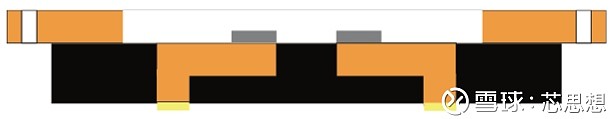
图1:预包封的MIS引线框架 来源:宇芯Unisem
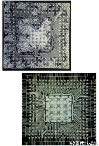
图2:基于MIS的IC封装 来源:Prismark,QDOS 表面上,MIS类似于扇出型(Fan-Out)晶圆级封装。它们之间最大的区别是,MIS在I/O和密度方面稍加逊色。因此,在实际封装使用中,MIS主要跟目前一些已经比较成熟的中端封装进行竞争。 MIS已经存在了近十年,但市场刚刚开始起来。“(MIS)由于其先进的布线能力和可靠性,在高、低功率应用上都很适用,” 日月光工程技术营销总监Mark Gerber说。 此外,MIS还为客户提供了一种新的封装选择,以及现有封装的一种潜在的替代方案。“出货量在这几年不断上升,”Nokibul Islam说。“可以用MIS来替代一些传统的如QFN封装或基于引线框的封装,因为MIS具有更细的布线能力,更优的电和热性能,和更小的外形。” 还有, MIS封装被锁定用于数字货币芯片的封装,进入了数字货币服务器市场。这个市场的量是非常巨大的。当然也有一些人开始考虑数字货币市场是否或者说何时可能结束。 什么是MIS? MIS是在2010年左右开发的,长电科技是最早期的开发者之一,然后将这项技术授权给其兄弟公司芯智联(MISpak)。 芯智联(MISpak)开发和销售MIS材料给封装厂(OSAT),其他MIS基板供应商还包括ASM、PPT、QDOS和SIMMTECH。 因此,封装厂购买MIS基板有更多的选择。然后,在封装过程中,把芯片放在MIS基板上进行封装,最后形成MIS封装。
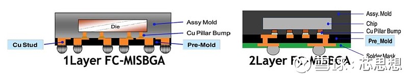
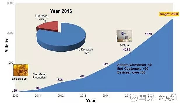
图3:矽品的倒装MIS BGA封装(FC-MISBGA) 来源:TechSearch International,矽品精密SPIL 随着时间的推移, MIS业务规模开始迅速成长。2017年,仅芯智联(MISpak)一家就预计出货25亿颗,而在2010年,其出货量仅2000万颗。在MIS封装领域,芯智联(MISpak)宣称其大约有30多家终端顾客。当然这中间还没包括其他MIS供应商的出货量。
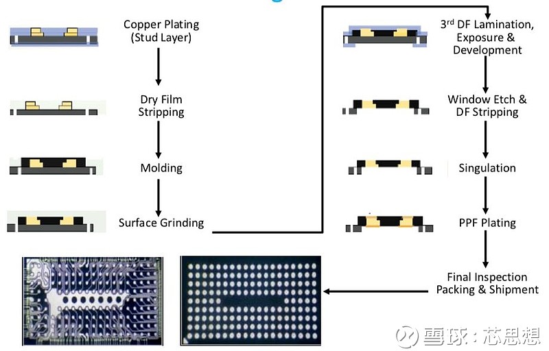
图4:芯智联MIS基板出货量 来源:芯智联MISpak MIS与传统 IC封装基板不同。传统封装采用的是有机基板,这是基于PCB类材料的多层基板技术。在封装中,芯片置于基板之上。 “MIS技术的特点是,它是从包封技术引申发展出来的。在MIS基板中,铜布线是嵌入式的。因此,这种嵌入式结构就可以做到更细的布线,” Nokibul Islam说。 MIS还具有其他的一些特性。“它使用包封料作为各层之间的绝缘材料,” Mark Gerber说。“当你使用该类型的引线框,并在此上进行封装,那么封装的包封料与引线框的材料特性就是相似的。因此,从吸潮性或功能的角度来看就非常好。” 目前制作MIS基板的方法有多种。MIS最早是以尺寸250mmX70mm的长条形出现 。MIS制作需要经过一系列的工艺步骤,如蚀刻、研磨、光刻、包封和电镀。 比如,单层MIS工艺流程,往往从载板开始。“在金属载板上,通过电镀铜来制作基板的布线,”Nokibul Islam解释道。“所以在完成电镀铜后,下一步就是去除光阻膜工艺。” 在去膜后。“就开始进行包封。然后研磨包封料进行减薄,达到所要求的厚度。最后蚀刻载板,”Nokibul Islam说。
图5:MIS基板制造工艺流程 来源:长电科技JCET 对于MIS封装,该技术最有优势的是薄型、I / O在150〜200之间的封装。但该技术受限于25μm左右的线宽线距,这意味着它主要面向中端应用。线宽线距是指封装中的金属布线。 对比来看,主要用于高端应用的扇出型封装(Fan-Out),其标准密度是: I / O小于500的封装,其线宽线距在8μm以上;而高密度扇出型封装,其I / O大于500,线宽线距小于8μm。 同时,MIS材料本身相对较薄。该类基板在封装过程中容易出现翘曲及均匀性问题。产量和成本问题则另论。 “不同的应用需求在设计灵活性和封装厚度方面需要特殊的封装材料,” ASM材料业务部市场副总裁Ho Kwok Kuen说。“相比引线框架,ABiT-MIS有能力可以生产出要求高、线路复杂的预包封基板。但是,为了达到设计的解析度需要更多的工艺步骤,因此为了达到最终产品的良率目标,我们需要高度关注在每一个工艺过程中如何实现更高的良率。” 除了设备,ASM也提供引线框架和MIS封装材料。这里是指ASM加层互连技术(ABiT,ASM Buildup Interconnect Technology )。 尽管面临种种挑战,但是MIS市场还是迅速成长。“在过去的两年里,我们已经看到了许多客户希望使用MIS封装来满足数字货币挖矿应用的需求。”Ho说,“MIS不仅在通讯领域射频封装的市场份额不断增加,其实在电源管理和汽车应用方面的需求也在不断增加。” 同时在市场上, MIS也是面临着激烈的竞争。这里指“Fan-Out”技术,尽管MIS并不会与Fan-Out技术竞争。其实MIS主要是与引线框封装和LGA封装进行竞争。“MIS的应用领域主要是介于标准QFN封装和简单的双层基板两者之间的封装。”宇芯北美区副总裁Gil Chiu说。 引线框封装包括若干封装类型,诸如四面扁平无引线(QFN)和四面扁平封装(QFP)。引线框是金属框架,芯片粘贴在框架上,使用细导线进行连接。
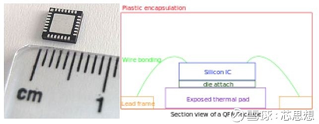
图6:QFN封装 来源:维基百科 QFN是成熟、价格低且可靠的封装方式,因此在模拟、汽车电子、物联网、RF等市场方面,QFN的需求巨大。通常来讲,虽然QFN是一个I / O能力有限的单层技术,但是“如果你可以用QFN实现,你显然会这么做,因为QFN的成本比MIS更低,”Chiu说。“但是当你使用QFN时,你要接受间距的限制。” MIS还与LGA封装技术竞争。LGA在封装底部有用于连接的金属焊盘阵列。LGA适用于模块、处理器等产品。
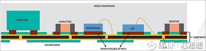
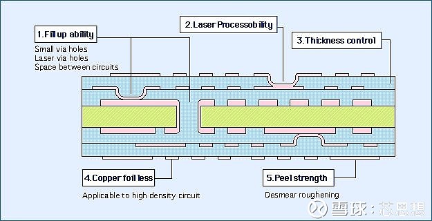
图7:电源模块LGA封装结构 来源:美信集成Maxim MIS的成本相比LGA更便宜,但是能力不足LGA。然而,宇芯公司认为LGA有时会受高昂的材料成本、连接孔(Via)成型成本等影响。 因此,QFN和LGA都有一些缺点,这里就是MIS的用武之地。例如,IC设计公司可能会在给定的工艺节点有现成的芯片设计,且芯片封装采用QFN封装。在这个假设的例子中,供应商会面临一些挑战。“客户基本上会说,我有一个现成的方案,我不想改变我的芯片,我不希望缩小我的芯片面积,但我希望改变我的封装外形,我希望得到一个更薄、更小尺寸的封装,”Chiu说。 一种有效的解决方案就是从QFN封装转向MIS封装。通常,你可以采用与引线框封装相同的芯片,用在MIS上进行封装。MIS封装可以做到跟QFN封装外形一致,但MIS可以有更多的 I / O和更好的性能。 采用MIS封装,基本上可以和其他封装类型一样,例如:倒装芯片、模块和SiP。“MIS技术是不同的。它本质上是一种积层工艺。它可以让你实现更密的金属布线。因此,您可以缩小封装,而同时保持相同的芯片尺寸,”Chiu说。“使用MIS,客户不必花费时间或资源来重新设计一个更小的芯片以及不必缩小芯片的外形。采用MIS,产品可以有更多方案选择,可以让产品管脚或产品接口保持不变。所以,MIS在相同的成本下可以为您提供更小的封装。” “搭上”或“错过”? 一段时间以来,OSAT厂商已经不断有MIS封装的产品出货。但是每个OSAT厂商都有不同的战略。 长电科技/星科金朋已经出货了各类基于MIS技术的Chip-on-lead、FC、模组及SiP封装产品。“MIS具有其特定的优势。最优的是低 I / O数的高功率、高散热的应用。” 长电科技的Islam说。 到目前为止,业内主要出货的是线宽线距在25/25μm的单层MIS封装。“对于未来的市场,我们目前正在做更高的解析度,这意味着更细的线宽线距,以及更轻薄的外形,”Islam说。“两年以后,它可以做到15/15μm的线宽线距。” 此外,长电科技/星科金朋以及其他厂商都在全力致力于基于Ajinomoto的ABF(Ajinomoto Build-up Film)膜技术的更先进的工艺。使用激光成型和直接电镀铜,ABF可以使MIS做到线宽线距达12/12μm的多层基板,这样可以实现二层、三层及四层的多层封装。
图8:Ajinomoto 的ABF膜的优势 来源:Ajinomoto “使用ABF膜,MIS的工艺流程基本完全是一样的。我们只是使用更厚的ABF膜来替代包封料,我们可以提供这种类型的多层MIS基板,”Islam说。“在今年年底左右我们就会开始使用基于ABF膜的两层或三层MIS基板。” 日月光的MIS封装也正在成长中。日月光的MIS技术被称为C2IM / MIS。“MIS可以让你做到型同QFN封装而同时具备精细节距布线能力的封装,” 日月光的Gerber说。“(有些客户)非常坚持使用QFN封装,但是有布线能力的限制。当你可以进行20/20μm或30/30μm的布线,这就一下子为他们提供了一层布线金属层的解决方案。” 除了C2IM / MIS,日月光还提供另一个竞争性的技术叫“ChipLast扇出封装”,这不同于现行的扇出型封装。“它本质上是一个芯片后置的工艺,这就意味着它是一个倒装芯片工艺,”Gerber说。“ChipLast扇出封装是一个根据布线密度使用两种不同绝缘材料,而只有一层金属布线的无芯基板工艺方案”。 此外,相对于MIS基板,日月光还有另一个选择方案叫做aS3 +。“aS3 +是一个嵌入式线路(ET)的无芯有机基板,这个技术也可以提供与C2IM / MIS类似优势的方案。此外,aS3 + / ET基板可以做到三层或更多层布线,而在这方面C2IM / MIS相对比较欠缺,”他说。“aS3 + / ET可以使用传统绝缘材料或ABF绝缘材料。同时由于不需要芯板材料以及其制造工艺流程和它内在的结构特点,它可以带来有利于更高速度连接的层间超低电感,同时不失成本竞争力及可靠性 ”。 对宇芯来讲,他们看到的是MIS封装的三个应用。这些封装都可以做到整体厚度达到0.33毫米或更低。 第一种应用是该公司所谓的空腔,芯片封装在这个封装体的空腔里。“我们正在利用MIS实现介于基板封装与QFN封装之间的细间距芯片倒装封装,在这方面可以一展身手,”宇芯的Chiu如是说。“我们同样还在考虑使用MIS进行系统级封装,这对于LGA标准模块封装来说,是一个成本更低的方案。” 对于MIS来说,最大的市场是电源/功率IC。另一个驱动因素是数字货币IC封装。展望未来,MIS可能会超出这些市场。“好消息是,我们看到越来越多的常规产品也在考虑是否使用MIS封装.”Chiu补充说。
MIS Packaging Takes Off Molded interconnect substrate emerges as packaging choice for analog, power ICs and cryptocurrency chips. Momentum is building for IC packages based on an emerging technology called molded interconnect substrate (MIS). ASE, Carsem, JCET/STATS ChipPAC, Unisem and others are developing IC packages based on MIS substrate technology, which is ramping up in the analog, power IC and even the cryptocurrency markets. MIS starts with a specialized substrate material for select IC packages. The MIS substrate itself is developed and sold by various vendors. A packaging house then takes that substrate and assembles an IC package around it. Some refer to the MIS substrate as a leadframe. MIS is different than traditional substrates, as the technology consists of a pre-molded structure with one or more layers. Each layer is pre-configured with copper plating or interconnects to provide electrical connections in the package. All told, MIS supports single- or multi-die configurations, enabling low-profile, fine-pitch packages. It can be used to develop souped-up leaded packages, flip-chip, modules and system-in-packages (SiPs). On the surface, MIS resembles a fan-out wafer-level package. The big difference is that MIS is limited in terms of I/Os and densities. So in reality, MIS competes in the midrange space against some well-entrenched package types. MIS has been around for nearly a decade, but the market is just starting to take off. “(MIS is) growing in both low- and high-power applications due to advanced routing and reliability properties,” said Mark Gerber, director of engineering and technical marketing at Advanced Semiconductor Engineering (ASE). In addition, MIS also presents customers with new options, as well as potential replacements for existing packages. “The volumes are increasing over time,” said Nokibul Islam, director of group technology strategy for the JCET Group of companies. “Some of the traditional QFN- or leadframe-based packages can be replaced with MIS because of the line and space capabilities, the electrical and thermal performance, and small form factors.” In addition, MIS-based packages are being targeted for house chips that go in the cryptocurrency server market. Potentially, the volumes are enormous, but many wonder if or when the cryptocurrency market will dry up. What is MIS? MIS was developed around 2010. JCET, one of the early developers of this approach, licensed the technology to a sister company called MISpak Technology. MISpak, in turn, develops and sells MIS substrates to outsourced assembly and test (OSAT) companies. Other companies, such as ASM Pacific Technology, PPT, Qdos and Simmtech, also sell MIS substrates. So, OSATs can buy MIS substrates from any number of vendors. Then, in the assembly process, OSATs would incorporate dies within in the MIS substrate, which then becomes the final package. Over time, the MIS business has taken off, as MISpak alone was projected to ship 2.5 billion units in 2017, up from roughly 20 million units in 2010. MISpak claims to have roughly 30 customers in the arena. This doesn’t include shipments from the other MIS players. MIS is different than traditional substrates for IC packaging. Many packages use organic substrates, which are multi-layer technologies based on PCB-like materials. In a package, dies are placed on the substrate. “The interesting feature of MIS technology is that it is made out of a mold compound. The copper traces in the MIS substrate are embedded. So with that, it allows you to have much finer line and space,” JCET’s Islam said.It also has other properties. “It uses mold compound as the dielectric in between the layers,” said ASE’s Gerber. “When you take that type of leadframe, and then you mold on top of that, the material properties between your mold compound and the leadframe are similar. So it performs very well from a moisture or performance perspective.” There are several ways to make an MIS substrate. MIS originally comes in the form of a strip measuring 250mm x 70mm. Then the MIS strip undergoes a series of process steps, such as etch, grinding, lithography, molding and plating. In a one-layer MIS flow, for example, the process starts with a carrier. “On the metal carrier, you do the copper plating to make the traces of the substrate,” Islam explained. “So it’s copper plating, followed by a dry film resist process.”The resist is stripped. “Then you apply the mold compound. Finally, you grind the mold compound to make sure it meets the desired thickness of the substrate. The last step is to etch the carrier from the panel,” he said. Fig. 5: MIS Substrate Manufacturing Process Flow Source: JCETFor MIS-based packages, the technology is ideal from 150 to 200 I/Os in low profiles. But the technology is limited to around 25μm line and space, meaning it is geared for mainly mid-range applications. Line and space refers to the width and pitch of a metal trace in a package. In comparison, a standard-density fan-out package, which is aimed for high-end apps, is defined as a package with less than 500 I/Os and greater than 8μm line/space. High-density fan-out has more than 500 I/Os and less than 8μm line/space. Meanwhile, the MIS substrate itself is thin. The substrate could be prone to warpage and uniformity issues during a process. Yield and cost are other issues. “Different applications require specific packaging material in design flexibility and package thickness,” said Ho Kwok Kuen, vice president of marketing in the Material Business segment at ASM Pacific Technology. “Compared to leadframes, ABiT-MIS is capable of producing demanding and complex circuit-designed molded substrates. There are, however, more process steps needed to achieve the design resolution, and we put high focus on achieving a higher yield at each of these individual processes in order to meet the targeted yield at the end of the production line.” Besides equipment, ASM Pacific Technology also provides leadframes and MIS packaging materials. It refers to these technologies as ASM Buildup Interconnect Technology (ABiT). Despite the challenges, MIS is growing. “In the last two years, we have seen a spike in interest from many customers looking to use this packaging platform for cryptocurrency mining applications. While MIS is seeing an increasing market share in RF components in telecommunications devices, there are also increasing enquiries from power management and automotive applications as well,” Ho said. In the market, meanwhile, MIS faces stiff competition. Some refer to the technology as “fan-out,” although MIS doesn’t compete with fan-out. Instead, MIS competes against leadframe-based packages and land grid arrays (LGAs). “The MIS space hovers between what I would call a standard leadless QFN package and a simple two-layer laminated substrate,” said Gil Chiu, vice president of North America at Unisem. The leadframe group consists of several packaging types, such as quad-flat no-lead (QFN) and quad flat-pack (QFP). A leadframe is a metal frame. A die is attached to the frame and connected using thin wires. QFN is mature, cheap and reliable, so there is enormous demand for QFN in analog, automotive, IoT, RF and other markets. Generally, though, QFN is a single-layer technology with limited I/O capabilities. “If you can put it in a QFN, you would obviously do it. A QFN has a lower cost than MIS,” Chiu said. “But when you talk about QFN, you have a limitation in how fine a pitch you can get.” MIS also competes against laminate packages like LGAs. LGAs consist of a grid of contacts on the underside of a package. LGAs are used for modules, processors and other products. MIS is cheaper but has less capabilities than LGAs. However, LGAs sometimes suffer from high material and via formation costs, according to Unisem. So, QFN and LGA have some shortcomings and that’s where MIS fits in. For example, an IC vendor might have an existing chip design at a given process node. The chip is housed in a QFN package. In this hypothetical example, the vendor faces some challenges. “A customer basically says, ‘I have a current solution. I don’t want to change my die. I don’t want to shrink my die. But I want to shrink the package. And I want to get to a low profile and a smaller size,’ ” Chiu said. One solution is to move from a QFN-based leadframe package to MIS. Generally, you can take the same die in a leadframe-based package and place it in an MIS substrate. The final MIS package resembles a QFN package, but MIS has more I/Os and better performance. With MIS, customers can essentially do the same thing with other package types, such as flip-chip, modules and SiPs. “MIS is different. It’s essentially a built-up process. It allows you to frame the metal traces closer. Therefore, you can shrink the package, while maintaining the same die size,” Chiu said. “(With MIS), the customer doesn’t have to spend time or resources to spin a smaller die and reduce the geometries at the die level. With MIS, you can get an extra life out of a product. It allows you to maintain a socket with a known solution. So MIS gives you a smaller package and still gives you the same cost structure.” Hit or MIS? For some time, several OSATs have shipped MIS-based packages. Each vendor has a different strategy. JCET/STATS, for one, has shipped chip-on-lead, flip-chip, modules and SiPs based on MIS technology. “MIS has certain sweet spots. Number one is for high-power, high-thermal applications, but for low I/O counts,” JCET’s Islam said. So far, the industry has mainly shipped single-layer MIS packages with 25-25μm line/space. “Moving forward, we are also working on finer resolutions. That means finer line and space, as well as much thinner form factors,” Islam said. “Two years down the road, it could go down to 15-15μm line and space.”In addition, JCET/STATS and others are gearing up for a more advanced process involving a so-called Ajinomoto Build-up Film (ABF) technology. Using laser processing and direct copper plating, ABF enables multiple layers in a substrate at 12-12μm. ABF enables two-, three- and four-layer packages. “(With ABF), the process flow is exactly the same. Instead of mold compound, we will be using a heavier film. We can have multiple layers of that type of substrate,” he said. “We expect to a start two- or three-layer MIS using ABF sometime at the end of the year.” ASE also is ramping up MIS-based packages. ASE’s MIS technology is called C2IM/MIS. “MIS allows you to do some routing in a fairly fine-pitch capability and in a QFN-like format,” ASE’s Gerber said. “(Some customers) have been stuck in QFN, which has limited routing capabilities. When you get a solution that you can actually route at 20-20μm or 30-30μm line/space, that opens up a lot of options for them for one metal layer.” Besides C2IM/MIS, ASE also offers a competitive technology called “Chip Last Fan Out.” This is not a fan-out wafer-level packaging, however. “It’s essentially a die last process, which means it’s a flip-chip process,” Gerber said. “Chip Last Fan Out is a one-metal layer coreless-based solution that uses two different dielectric materials depending on the routing density.” In addition, ASE has an alternative to an MIS substrate, dubbed AS3+. “AS3+ is an embedded trace (ET) coreless organic substrate that can offer some similar benefits as the C2IM/MIS solution. In addition, the AS3+/ET substrate allows for three or more routing layers where C2IM/MIS may be limited,” he said. “AS3+/ET may use traditional or ABF dielectric materials. And due to the lack of a core material, it can offer ultra-low inductance between layers to benefit higher speed connections while being cost competitive and reliable due to its manufacturing process flow and its inherent structure.” For its part, Unisem sees a trio of applications for MIS packages. These packages have an overall thickness of 0.33mm or lower.The first application is what the company calls air cavity, where a single die is situated inside a package. “We are also using MIS for fine-pitch flip-chip solutions as a go between a laminate versus QFN,” Unisem’s Chiu said. “We are also thinking about doing system-in-package using MIS. It’s a lower cost option to an LGA standard module package.”For MIS, the big market is power ICs. Another driver is IC packages in cryptocurrency. And going forward, MIS may expand beyond those markets. “The good news is that we are seeing a lot more standard products looking at it,” Chiu added. |

 以下为英文原文
【本文地址】