| sram设计流程+memory compiler整理 | 您所在的位置:网站首页 › 升级win11需要开启什么 › sram设计流程+memory compiler整理 |
sram设计流程+memory compiler整理
|
1. 设计流程的介绍
先设计出电路图schematic
→
\rightarrow
→进行仿真用ADE
→
\rightarrow
→画出版图layout
→
\rightarrow
→使用claibre做DRC和LVS
→
\rightarrow
→寄生参数提取,后仿真。(参考见此)
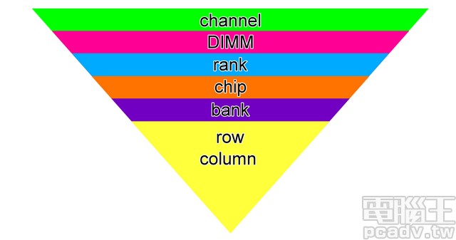
ADE是analog design environment的缩写,是virtuoso的一个对电路schematic的仿真工具,用于前仿真阶段,后仿真好像也用得到(在virtuoso514版本里是analog environment,而在617版本里它就变成了ADE缩写,在launch里能找到这个工具。 DRC是用你绘制的版图和工艺规则做对比,工艺规则一般由代工厂提供,用来检查版图绘制是否符合标准的。 LVS—layout vs schematic,即版图和电路图进行比对,看看版图绘制是否和电路图的连接关系一致,这个是使用版图的网表和电路图的网表做对比的,但是也是需要lvs规则的。 2. Memory compiler(储存器编译器)在半导体设计领域,存储器编译器是用于自动设计和生成集成电路 (IC) 中使用的存储器电路的过程的软件工具。这些存储器电路可以包括静态随机存取存储器(SRAM)、只读存储器(ROM)和动态随机存取存储器(DRAM)等。取自anysilicon 内存编译器的工作原理是获取内存大小、速度、功耗和时序约束等输入参数,并生成满足这些规范的内存电路布局。与手动设计存储器电路相比,这种自动化过程可以节省时间和资源,并且还有助于确保不同存储器设计之间的一致性和可靠性。 Memory compilers work by taking input parameters such as memory size, speed, power consumption, and timing constraints and generating a memory circuit layout that meets these specifications. This automated process saves time and resources compared to manually designing memory circuits, and also helps ensure consistency and reliability across different memory designs. 内存编译器提供了一种自动化方法,可以根据各种输入参数(例如字数、位数、外围阈值电压、列复用器比率、存储体数量等)生成自定义 SRAM 实例,并针对面积和功耗进行了优化。我们将详细讨论这些参数。 下图是一个一般情况下的一个memory core的概略图。 [外链图片转存失败,源站可能有防盗链机制,建议将图片保存下来直接上传(img-BvXgU4AO-1687918689835)(https://anysilicon.com/wp-content/uploads/2023/05/mem-complier-pic2-1024x904.png)] Memory Compiler Types Trade off between Speed and Density. 速度快,面积会比较大,你面积小,速度会比较慢,因此需要在这两个方面之间进行抉择。是HS(High speed)还是HD (High density)。 体系结构:以下是基于体系结构规范的常用内存编译器: 单端口存储器:单端口存储器支持一个时钟周期内的一次读取或一次写入操作。两个端口存储器:两个端口存储器支持一个时钟周期内的一次读取或一次写入或一次读取和一次写入操作。双端口存储器:双端口存储器支持在一个时钟周期内进行两次读取或两次写入或一次读取和一次写入操作。这些 SRAM 有两个时钟引脚:一根用于读取,一根用于写入。These SRAMs have two clock pins: one for read and one for write. Architecture: Following are the commonly used memory compilers based on the architectural specification: Single Port Memories: Single port memories support one read OR one write operation in a clock cycle.Two Port Memories: Two port memories support one read OR one write OR one read and one write operation in a clock cycle.Dual Port Memories: Dual port memories support two read OR two write OR one read and one write operation in a clock cycle. These SRAMs have two clock pins: one for read and one for write. Number of WordsThe functional or the size of the memory is specified in the form of number of words. 存储器的功能或大小以字数的形式指定。 Number of Bits per Word (BPW)Bits per word specify the number of bits per word in a given functional specification of the SRAM. It is worth nothing that the number of words and number of bits per word are only the functional specification. Physically, any SRAM is arranged in the form of rows and columns. 每字位数指定 SRAM 给定功能规范中每字的位数。毫无意义的是,字数和每个字的位数只是功能规格。物理上,任何 SRAM 都是以行和列的形式排列的。 VT TypeVT type specifies the threshold voltage of the transistors used to implement a given memory. This should be: HVT: High VT offering slower access time and low leakage. LVT: Low VT offering faster access time and high leakage. Ultra-LVT: Very low VT offering fastest access time at the cost of very high leakage. MVT: Mixed VT offering the right balance between access times and the leakage power. Number of Banks下面的图是表示了一个memory的结构,从大到小分别是channel,DIMM,rank,chip,bank,row column。
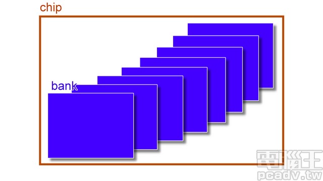
下面这张图是描述了bank和chip的关系。其实bank就是相当是很多储存单元的组合,然后到底是几行几列是要看具体的设计来决定的。
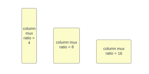
Some compilers also support the option of more than 1 banks (bit array banks) that allows the maximum capacity of the compiled SRAM to effectively increase. Multi-bank memories use symmetrical placement of the banks to share the peripheral circuitry in such a way that the access times to any individual bank is uniform. Multi-bank memories are more area efficient as multiple banks share the same circuitry. In addition to the area, multi-bank memories also provide the option to put the individual banks into a lower power mode to conserve leakage power. Aspect RatioDesigners are given the option to control the aspect ratio of the physical SRAM that works well for their floorplan. This is accomplished with the help of “column mux ratio”, where a lower value of column mux ratio results in taller memories while a higher value results in flatter memories. 设计人员可以选择控制适合其布局规划的物理 SRAM 的纵横比。这是在“列复用器比率”的帮助下完成的,其中较低的列复用器比率值会导致更高的存储器,而较高的值会导致更平坦的存储器。
Power dissipation is quite a big concern, and memory compilers support following low power modes: Nap(小睡): SRAM is said to be in nap state when the periphery supply is turned off while the core supply is still on. This mode helps conserve leakage power. Retention(滞留,维持): This option saves the memory states in a low power mode when the SRAM is in the power down enable mode. This mode is similar to that of a state retention power gating. In this mode, the core voltage is maintained at a minimum voltage value to retain the data. Shutdown: In the shutdown mode, both the periphery supply and the core supply are switched off. The contents of the SRAM are lost, and this state has the lowest leakage power consumption. Since both the supplies are switched off, waking up from this state takes the longest (wake up time). Memory Compiler OutputsMemory compiler outputs the following files to be used downstream by physical design and other flows: Netlist: Memory Compiler generates a netlist of the generated memory that is read by the physical design tools and needed while running the Layout versus Schematic (LVS) check and also needed during functional verification of the design. Layout Extraction Format (LEF): This is the layout model of the SRAM used for physical placement and during extraction. Timing Models: These are the liberty files that contains all the timing information for synthesis, static timing analysis (STA) and gate level simulations (GLS). Based on all the scenarios enabled while running memory compiler, it generates a .lib for each requested scenario. Schematic: This is again needed for the LVS check. Symbol: This is needed for schematic capture. Memory Datasheet: This offers an easy-to-read summary of the key timing and area numbers of the memory across multiple scenarios. AVM Models: AVM models are required by the EM/IR tool to perform power integrity signoff checks like static IR drop, dynamic IR drop etc. These files contain the current numbers for every mode like the read or write or read/write, leakage current numbers, the decoupling capacitance numbers, the SDF conditions and the output load assumed for each output pin. EM/IR tools use this information to deduce the current waveform at the SRAM power pins to subsequently use them for voltage drop analysis. each output pin. EM/IR tools use this information to deduce the current waveform at the SRAM power pins to subsequently use them for voltage drop analysis. 后续阅读arm compiler |
【本文地址】