| Micromachines | 您所在的位置:网站首页 › mdpi期刊目录下载 › Micromachines |
Micromachines
|
Journals
Active Journals
Find a Journal
Proceedings Series
Topics
Information
For Authors
For Reviewers
For Editors
For Librarians
For Publishers
For Societies
For Conference Organizers
Open Access Policy
Institutional Open Access Program
Special Issues Guidelines
Editorial Process
Research and Publication Ethics
Article Processing Charges
Awards
Testimonials
Author Services
Initiatives
Sciforum
MDPI Books
Preprints.org
Scilit
SciProfiles
Encyclopedia
JAMS
Proceedings Series
About
Overview
Contact
Careers
News
Press
Blog
Sign In / Sign Up
Notice
clear
Notice
You are accessing a machine-readable page. In order to be human-readable, please install an RSS reader. Continue Cancel clearAll articles published by MDPI are made immediately available worldwide under an open access license. No special permission is required to reuse all or part of the article published by MDPI, including figures and tables. For articles published under an open access Creative Common CC BY license, any part of the article may be reused without permission provided that the original article is clearly cited. For more information, please refer to https://www.mdpi.com/openaccess. Feature papers represent the most advanced research with significant potential for high impact in the field. A Feature Paper should be a substantial original Article that involves several techniques or approaches, provides an outlook for future research directions and describes possible research applications. Feature papers are submitted upon individual invitation or recommendation by the scientific editors and must receive positive feedback from the reviewers. Editor’s Choice articles are based on recommendations by the scientific editors of MDPI journals from around the world. Editors select a small number of articles recently published in the journal that they believe will be particularly interesting to readers, or important in the respective research area. The aim is to provide a snapshot of some of the most exciting work published in the various research areas of the journal. Original Submission Date Received: .  4.7
4.7

 3.4
Journals
Micromachines
3.4
Journals
Micromachines
 Chameleon-Inspired Colorimetric Sensors for Real-Time Detections with Humidity
 Polarization Z-Scan Studies Revealing Plasmon Coupling Enhancement Due to Dimer Formation of Gold Nanoparticles in Nematic Liquid Crystals
 Controllable Carrier Doping in Two-Dimensional Materials Using Electron-Beam Irradiation and Scalable Oxide Dielectrics
 Acoustic Bubble and Magnetic Actuation-Based Microrobot for Enhanced Multiphase Drug Delivery Efficiency
Journal Description
Micromachines
Micromachines
is a peer-reviewed, open access journal on the science and technology of small structures, devices and systems, published monthly online by MDPI.
Open Access— free for readers, with article processing charges (APC) paid by authors or their institutions.
High Visibility: indexed within Scopus, SCIE (Web of Science), PubMed, PMC, Ei Compendex, dblp, and other databases.
Journal Rank: JCR - Q2 (Chemistry, Analytical) / CiteScore - Q2 (Mechanical Engineering)
Rapid Publication: manuscripts are peer-reviewed and a first
decision is provided to authors approximately 16.1 days after submission; acceptance
to publication is undertaken in 1.9 days (median values for papers published in
this journal in the second half of 2023).
Recognition of Reviewers: reviewers who provide timely, thorough peer-review reports receive vouchers entitling them to a discount on the APC of their next publication in any MDPI journal, in appreciation of the work done.
Testimonials: See what our editors and authors say about Micromachines.
Impact Factor:
3.4 (2022);
5-Year Impact Factor:
3.3 (2022)
subject
Imprint Information
get_app
Journal Flyer
Open Access
ISSN: 2072-666X
Latest Articles
11 pages, 3730 KiB
Open AccessArticle
Breakdown Characteristics of GaN DMISFETs Fabricated via Mg, Si and N Triple Ion Implantation
by
Acoustic Bubble and Magnetic Actuation-Based Microrobot for Enhanced Multiphase Drug Delivery Efficiency
Journal Description
Micromachines
Micromachines
is a peer-reviewed, open access journal on the science and technology of small structures, devices and systems, published monthly online by MDPI.
Open Access— free for readers, with article processing charges (APC) paid by authors or their institutions.
High Visibility: indexed within Scopus, SCIE (Web of Science), PubMed, PMC, Ei Compendex, dblp, and other databases.
Journal Rank: JCR - Q2 (Chemistry, Analytical) / CiteScore - Q2 (Mechanical Engineering)
Rapid Publication: manuscripts are peer-reviewed and a first
decision is provided to authors approximately 16.1 days after submission; acceptance
to publication is undertaken in 1.9 days (median values for papers published in
this journal in the second half of 2023).
Recognition of Reviewers: reviewers who provide timely, thorough peer-review reports receive vouchers entitling them to a discount on the APC of their next publication in any MDPI journal, in appreciation of the work done.
Testimonials: See what our editors and authors say about Micromachines.
Impact Factor:
3.4 (2022);
5-Year Impact Factor:
3.3 (2022)
subject
Imprint Information
get_app
Journal Flyer
Open Access
ISSN: 2072-666X
Latest Articles
11 pages, 3730 KiB
Open AccessArticle
Breakdown Characteristics of GaN DMISFETs Fabricated via Mg, Si and N Triple Ion Implantation
by
 Tohru Nakamura, Michitaka Yoshino, Toru Toyabe and Akira Yasuda
Micromachines 2024, 15(1), 147; https://doi.org/10.3390/mi15010147 - 18 Jan 2024
Abstract
Mg-ion-implanted layers in a GaN substrate after annealing were investigated. Implanted Mg atoms precipitated along the edges of crystal defects were observed using 3D-APT. The breakdown characteristics of a GaN double-diffused vertical MISFET (DMISFET) fabricated via triple ion implantation are presented. A DMISFET
[...] Read more.
Mg-ion-implanted layers in a GaN substrate after annealing were investigated. Implanted Mg atoms precipitated along the edges of crystal defects were observed using 3D-APT. The breakdown characteristics of a GaN double-diffused vertical MISFET (DMISFET) fabricated via triple ion implantation are presented. A DMISFET with Si-ion-implanted source regions was formed in Mg-ion-implanted p-base regions, which were isolated from adjacent devices by N-ion-implanted edge termination regions. A threshold voltage of −0.5 V was obtained at a drain voltage of 0.5 V for the fabricated vertical MISFET with an estimated Mg surface concentration of 5 × 1018 cm−3. The maximum drain current and maximum transconductance in a saturation region of Vds = 100 V were 2.8 mA/mm and 0.5 mS/mm at a gate voltage of 15 V, respectively. The breakdown voltage in the off-state was 417 V. The breakdown points were determined by the boundary regions between the N- and Mg-implanted regions. By improving heat annealing methods, ion-implanted GaN DMISFETs can be a promising candidate for future high-voltage and high-power applications.
Full article
(This article belongs to the Special Issue Low Energy, Focused Beam Ion Implantation for Semiconducting Materials and Devices)
►▼
Show Figures Tohru Nakamura, Michitaka Yoshino, Toru Toyabe and Akira Yasuda
Micromachines 2024, 15(1), 147; https://doi.org/10.3390/mi15010147 - 18 Jan 2024
Abstract
Mg-ion-implanted layers in a GaN substrate after annealing were investigated. Implanted Mg atoms precipitated along the edges of crystal defects were observed using 3D-APT. The breakdown characteristics of a GaN double-diffused vertical MISFET (DMISFET) fabricated via triple ion implantation are presented. A DMISFET
[...] Read more.
Mg-ion-implanted layers in a GaN substrate after annealing were investigated. Implanted Mg atoms precipitated along the edges of crystal defects were observed using 3D-APT. The breakdown characteristics of a GaN double-diffused vertical MISFET (DMISFET) fabricated via triple ion implantation are presented. A DMISFET with Si-ion-implanted source regions was formed in Mg-ion-implanted p-base regions, which were isolated from adjacent devices by N-ion-implanted edge termination regions. A threshold voltage of −0.5 V was obtained at a drain voltage of 0.5 V for the fabricated vertical MISFET with an estimated Mg surface concentration of 5 × 1018 cm−3. The maximum drain current and maximum transconductance in a saturation region of Vds = 100 V were 2.8 mA/mm and 0.5 mS/mm at a gate voltage of 15 V, respectively. The breakdown voltage in the off-state was 417 V. The breakdown points were determined by the boundary regions between the N- and Mg-implanted regions. By improving heat annealing methods, ion-implanted GaN DMISFETs can be a promising candidate for future high-voltage and high-power applications.
Full article
(This article belongs to the Special Issue Low Energy, Focused Beam Ion Implantation for Semiconducting Materials and Devices)
►▼
Show Figures
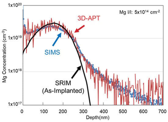 Figure 1 attachment Supplementary material: Supplementary File 1 (ZIP, 515 KiB) 12 pages, 2951 KiB Open AccessArticle Highly Transparent Red Organic Light-Emitting Diodes with AZO/Ag/AZO Multilayer Electrode byDongwoon Lee, Min Seok Song, Yong Hyeok Seo, Won Woo Lee, Young Woo Kim, Minseong Park, Ye Ji Shin, Sang Jik Kwon, Yongmin Jeon and Eou-Sik Cho
Micromachines 2024, 15(1), 146; https://doi.org/10.3390/mi15010146 - 18 Jan 2024
Abstract
Free-form factor optoelectronics is becoming more important for various applications. Specifically, flexible and transparent optoelectronics offers the potential to be adopted in wearable devices in displays, solar cells, or biomedical applications. However, current transparent electrodes are limited in conductivity and flexibility. This study
[...] Read more.
Free-form factor optoelectronics is becoming more important for various applications. Specifically, flexible and transparent optoelectronics offers the potential to be adopted in wearable devices in displays, solar cells, or biomedical applications. However, current transparent electrodes are limited in conductivity and flexibility. This study aims to address these challenges and explore potential solutions. For the next-generation transparent conductive electrode, Al-doped zinc oxide (AZO) and silver (AZO/Ag/AZO) deposited by in-line magnetron sputtering without thermal treatment was investigated, and this transparent electrode was used as a transparent organic light-emitting diode (OLED) anode to maximize the transparency characteristics. The experiment and simulation involved adjusting the thickness of Ag and AZO and OLED structure to enhance the transmittance and device performance. The AZO/Ag/AZO with Ag of 12 nm and AZO of 32 nm thickness achieved the results of the highest figure of merit (FOM) (Φ550 = 4.65 mΩ−1) and lowest roughness. The full structure of transparent OLED (TrOLED) with AZO/Ag/AZO anode and Mg:Ag cathode reached 64.84% transmittance at 550 nm, and 300 cd/m2 at about 4 V. The results demonstrate the feasibility of adopting flexible substrates, such as PET, without the need for thermal treatment. This research provides valuable insights into the development of transparent and flexible electronic devices.
Full article
(This article belongs to the Special Issue Organic Semiconductors and Devices)
►▼
Show Figures
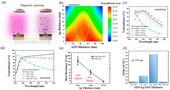 Figure 1 11 pages, 8072 KiB Open AccessArticle A Study on the Surface Quality and Damage Properties of Single-Crystal Silicon Using Different Post-Treatment Processes byWei Li, Fangyuan Zha, Bo Fu, Yanglong Li, Jiazhu Duan and Ziyou Zhou
Micromachines 2024, 15(1), 145; https://doi.org/10.3390/mi15010145 - 17 Jan 2024
Abstract
Detecting subsurface defects in optical components has always been challenging. This study utilizes laser scattering and photothermal weak absorption techniques to detect surface and subsurface nano-damage precursors of single-crystal silicon components. Based on laser scattering and photothermal weak absorption techniques, we successfully establish
[...] Read more.
Detecting subsurface defects in optical components has always been challenging. This study utilizes laser scattering and photothermal weak absorption techniques to detect surface and subsurface nano-damage precursors of single-crystal silicon components. Based on laser scattering and photothermal weak absorption techniques, we successfully establish the relationship between damage precursors and laser damage resistance. The photothermal absorption level is used as an important parameter to measure the damage resistance threshold of optical elements. Single-crystal silicon elements are processed and post-processed optimally. This research employs dry etching and wet etching techniques to effectively eliminate damage precursors from optical components. Additionally, detection techniques are utilized to comprehensively characterize these components, resulting in the successful identification of optimal damage precursor removal methods for various polishing types of single-crystal silicon components. Consequently, this method efficiently enhances the damage thresholds of optical components.
Full article
►▼
Show Figures
 Figure 1 attachment Supplementary material: Supplementary File 1 (ZIP, 701 KiB) 18 pages, 3758 KiB Open AccessArticle Miniaturization of CRISPR/Cas12-Based DNA Sensor Array by Non-Contact Printing byHiroki Shigemori, Satoshi Fujita, Eiichi Tamiya and Hidenori Nagai
Micromachines 2024, 15(1), 144; https://doi.org/10.3390/mi15010144 - 17 Jan 2024
Abstract
DNA microarrays have been applied for comprehensive genotyping, but remain a drawback in complicated operations. As a solution, we previously reported the solid-phase collateral cleavage (SPCC) system based on the clustered regularly interspaced short palindromic repeat/CRISPR-associated protein 12 (CRISPR/Cas12). Surface-immobilized Cas12-CRISPR RNA (crRNA)
[...] Read more.
DNA microarrays have been applied for comprehensive genotyping, but remain a drawback in complicated operations. As a solution, we previously reported the solid-phase collateral cleavage (SPCC) system based on the clustered regularly interspaced short palindromic repeat/CRISPR-associated protein 12 (CRISPR/Cas12). Surface-immobilized Cas12-CRISPR RNA (crRNA) can directly hybridize target double-stranded DNA (dsDNA) and subsequently produce a signal via the cleavage of single-stranded DNA (ssDNA) reporter immobilized on the same spot. Therefore, SPCC-based multiplex dsDNA detection can be performed easily. This study reports the miniaturization of SPCC-based spots patterned by a non-contact printer and its performance in comprehensive genotyping on a massively accumulated array. Initially, printing, immobilization, and washing processes of Cas12–crRNA were established to fabricate the non-contact-patterned SPCC-based sensor array. A target dsDNA concentration response was obtained based on the developed sensor array, even with a spot diameter of 0.64 ± 0.05 mm. Also, the limit of detection was 572 pM, 531 pM, and 3.04 nM with 40, 20, and 10 nL-printing of Cas12–crRNA, respectively. Furthermore, the sensor array specifically detected three dsDNA sequences in one-pot multiplexing; therefore, the feasibility of comprehensive genotyping was confirmed. These results demonstrate that our technology can be miniaturized as a CRISPR/Cas12-based microarray by using non-contact printing. In the future, the non-contact-patterned SPCC-based sensor array can be applied as an alternative tool to DNA microarrays.
Full article
(This article belongs to the Section B1: Biosensors)
►▼
Show Figures
 Figure 1 21 pages, 11882 KiB Open AccessArticle Radiation Detector Front-End Readout Chip with Nonbinary Successive Approximation Register Analog-to-Digital Converter for Wearable Healthcare Monitoring Applications byHsuan-Lun Kuo and Shih-Lun Chen
Micromachines 2024, 15(1), 143; https://doi.org/10.3390/mi15010143 - 17 Jan 2024
Abstract
A 16-channel front-end readout chip for a radiation detector is designed for portable or wearable healthcare monitoring applications. The proposed chip reads the signal of the radiation detector and converts it into digital serial-out data by using a nonbinary successive approximation register (SAR)
[...] Read more.
A 16-channel front-end readout chip for a radiation detector is designed for portable or wearable healthcare monitoring applications. The proposed chip reads the signal of the radiation detector and converts it into digital serial-out data by using a nonbinary successive approximation register (SAR) analog-to-digital converter (ADC) that has a 1-MS/s sampling rate and 10-b resolution. The minimum-to-maximum differential and integral nonlinearity are measured as −0.32 to 0.33 and −0.43 to 0.37 least significant bits, respectively. The signal-to-noise-and-distortion ratio and effective number of bits are 57.41 dB and 9.24 bits, respectively, for an input frequency of 500 kHz and a sampling rate of 1 MS/s. The SAR ADC has a 38.9-fJ/conversion step figure of merit at the sampling rate of 1 MS/s. The proposed chip can read input signals with peak currents ranging from 20 to 750 μA and convert the analog signal into a 10-bit serial-output digital signal. The input dynamic range is 2–75 pC. The resolution of the peak current is 208.3 nA. The chip, which has an area of 1.444 mm × 10.568 mm, is implemented using CMOS 0.18-μm 1P6M technology, and the power consumption of each channel is 19 mW. This design is suitable for wearable devices, especially biomedical devices.
Full article
(This article belongs to the Special Issue Bioelectronics and Wearable Devices: Sensing, Signal Processing and Powering, 2nd Edition)
►▼
Show Figures
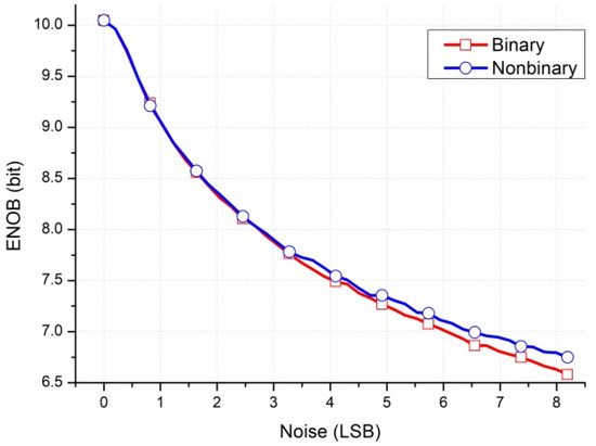 Figure 1 17 pages, 4852 KiB Open AccessArticle A Novel Compact Broadband Quasi-Twisted Branch Line Coupler Based on a Double-Layered Microstrip Line byFayyadh H. Ahmed, Rola Saad and Salam K. Khamas
Micromachines 2024, 15(1), 142; https://doi.org/10.3390/mi15010142 - 17 Jan 2024
Abstract
A novel quasi-twisted miniaturized wideband branch line coupler (BLC) is proposed. The design is based on bisecting the conventional microstrip line BLC transversely and folding bisected sections on double-layered substrates with a common ground plane in between. The input and output terminals, each
[...] Read more.
A novel quasi-twisted miniaturized wideband branch line coupler (BLC) is proposed. The design is based on bisecting the conventional microstrip line BLC transversely and folding bisected sections on double-layered substrates with a common ground plane in between. The input and output terminals, each with a length of λg/4, and the pair of quarter-wavelength horizontal parallel arms are converted into a Z-shaped meandered microstrip line in the designed structure. Conversely, the pair of quarter-wavelength vertical arms are halved into two lines and transformed into a periodically loaded slow-wave structure. The bisected parts of the BLC are placed on the opposite side of the doubled-layer substrate and connected through four vias passing through the common ground plane. This technique enabled a compact BLC size of 6.4 × 18 mm2, which corresponds to a surface area miniaturization by ~50% as compared to the classical BLC size of 10 × 23 mm2 at 6 GHz. Moreover, the attained relative bandwidth is 73.9% (4.6–10 GHz) for S11, S33, S21, and the phase difference between outputs (∠S21 − ∠S41). However, if a coupling parameter (S41) of up to −7.5 dB is considered, then the relative bandwidth reduces to 53.9% (4.6–10 GHz) for port 1 as the input. Similarly, for port 3 as the input, the obtained bandwidth is 75.8% (4.5–10 GHz) for S33, S11, S43, and the phase difference between outputs (∠S43 − ∠S23). Likewise, this bandwidth reduces to 56% (4.5–8 GHz) when a coupling parameter (S23) of up to −7.5 dB is considered. In contrast, the relative bandwidth for the ordinary BLC is 41% at the same resonant frequency. The circuit is constructed on a double-layered low-cost FR4 substrate with a relative permittivity of 4.3 and a loss tangent of 0.025. An isolation of −13 dB was realized in both S13 and S31 demonstrating an excellent performance. The transmission coefficients between input/output ports S21, S41, S23, and S43 are between −3.1 dB to −3.5 dB at a frequency of 6 GHz. Finally, the proposed BLC provides phase differences between output ports of 90.5° and 94.8° at a frequency of 6 GHz when the input ports 1 and 3 are excited, respectively. The presented design offers the potential of being utilized as a unit cell for building a Butler matrix (BM) for sub-6 GHz 5G beamforming networks.
Full article
(This article belongs to the Special Issue Recent Advances in Electromagnetic Devices)
►▼
Show Figures
 Figure 1 attachment Supplementary material: Supplementary File 1 (ZIP, 472 KiB) 10 pages, 1209 KiB Open AccessArticle Micromotors of MnO2 for the Recovery of Microplastics by Oscar Cervantes,Claudia Valtierra-Montiel, Laura Sampedro-Plata, Norberto Casillas, Nieves Menendez and Pilar Herrasti
Micromachines 2024, 15(1), 141; https://doi.org/10.3390/mi15010141 - 17 Jan 2024
Abstract
Plastics, primarily microplastics, are among the greatest pollutants in aquatic environments. Their removal and/or degradation in these environments are crucial to ensure an optimal future of these ecosystems. In this work, MnO2 particles were synthesized and characterized for the removal of polystyrene
[...] Read more.
Plastics, primarily microplastics, are among the greatest pollutants in aquatic environments. Their removal and/or degradation in these environments are crucial to ensure an optimal future of these ecosystems. In this work, MnO2 particles were synthesized and characterized for the removal of polystyrene microplastics as a model. MnO2 catalyzes the peroxide reaction, resulting in the formation of oxygen bubbles that propel the pollutants to the surface, achieving removal efficiencies of up to 80%. To achieve this, hydrothermal synthesis was employed using various methods. Parameters such as MnO2, pH, microplastics, and H2O2 concentrations were varied to determine the optimal conditions for microplastics recovering. The ideal conditions for a low microplastic concentrations (10 mg L−1) are 0.2 g L−1 MnO2, 1.6% of H2O2 and 0.01 triton as a surfactant. In these conditions, the micromotors can recover approximately 80% of 300 nm sized polystyrene microplastic within 40 min.
Full article
(This article belongs to the Special Issue Fundamentals and Catalytic Applications of Oxide-Based Materials)
►▼
Show Figures
 Figure 1 12 pages, 4533 KiB Open AccessArticle Air Gap Fiber Bragg Grating for Simultaneous Strain and Temperature Measurement byFuling Yang, Kehui Zhu, Xiaoyi Yu, Tianze Liu, Ke Lu, Zelong Wang and Yan Li
Micromachines 2024, 15(1), 140; https://doi.org/10.3390/mi15010140 - 16 Jan 2024
Abstract
We propose an air gap fiber Bragg grating (g-FBG) sensor that can measure strain and temperature simultaneously. The sensor is made by aligning two fiber Bragg gratings (FBGs), and an air gap exists between these two sub-gratings. This sensor’s architecture allows it to
[...] Read more.
We propose an air gap fiber Bragg grating (g-FBG) sensor that can measure strain and temperature simultaneously. The sensor is made by aligning two fiber Bragg gratings (FBGs), and an air gap exists between these two sub-gratings. This sensor’s architecture allows it to form a spectrum with phase-shifted fiber Bragg grating (PSFBG) spectroscopy and Fabry–Perot interference (FPI) spectroscopy. Since the sensitivity of PSFBG and FPI spectra is different for strain and temperature, it is possible to measure both strain and temperature by measuring one of the reflected dips of PSFBG and the interference dip of FPI. The experimental results show that the strain sensitivity is about 11.95 pm/με via the dip wavelength detection of FPI, and the temperature sensitivity is about 9.64 pm/°C via the dip wavelength detection of PSFBG. The g-FBG sensor demonstrates a resolution of approximately ±3.7 με within the strain range of 0 to 1000 με and about ±0.6 °C within the temperature range of 25 °C to 120 °C. The proposed g-FBG sensor, characterized by its simple structure, compact size, and cost-effectiveness, exhibits significant potential in the field of multi-parameter measurements.
Full article
►▼
Show Figures
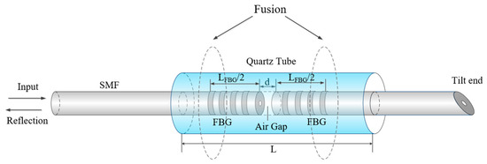 Figure 1 17 pages, 29594 KiB Open AccessArticle Theoretical and Experimental Investigation of Surface Textures in Vibration-Assisted Micro Milling byBowen Song, Dawei Zhang, Xiubing Jing, Yingying Ren, Yun Chen and Huaizhong Li
Micromachines 2024, 15(1), 139; https://doi.org/10.3390/mi15010139 - 16 Jan 2024
Abstract
Vibration-assisted micro milling is a promising technique for fabricating engineered mi-cro-scaled surface textures. This paper presents a novel approach for theoretical modeling of three-dimensional (3D) surface textures produced by vibration-assisted micro milling. The proposed model considers the effects of tool edge geometry, minimum
[...] Read more.
Vibration-assisted micro milling is a promising technique for fabricating engineered mi-cro-scaled surface textures. This paper presents a novel approach for theoretical modeling of three-dimensional (3D) surface textures produced by vibration-assisted micro milling. The proposed model considers the effects of tool edge geometry, minimum uncut chip thickness (MUCT), and material elastic recovery. The surface texture formation under different machining parameters is simulated and analyzed through mathematical modeling. Two typical surface morphologies can be generated: wave-type and fish scale-type textures, depending on the phase difference between tool paths. A 2-degrees-of-freedom (2-DOF) vibration stage is also developed to provide vibration along the feed and cross-feed directions during micro-milling process. Micro-milling experiments on copper were carried out to verify the ability to fabricate controlled surface textures using the vibration stage. The simulated and experimentally generated surfaces show good agreement in geometry and dimensions. This work provides an accurate analytical model for vibration-assisted micro-milling surface generation and demonstrates its feasibility for efficient, flexible texturing.
Full article
(This article belongs to the Special Issue Research Progress of Ultra-Precision Micro-Nano Machining)
►▼
Show Figures
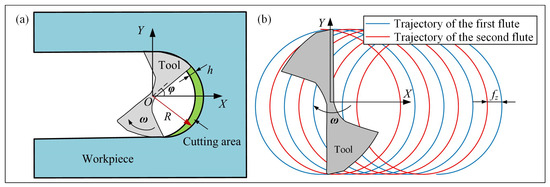 Figure 1 12 pages, 6504 KiB Open AccessArticle Thermal Conductivity Gas Sensors for High-Temperature Applications byNikolay Samotaev, Boris Podlepetsky, Mikhail Mashinin, Igor Ivanov, Ivan Obraztsov, Konstantin Oblov and Pavel Dzhumaev
Micromachines 2024, 15(1), 138; https://doi.org/10.3390/mi15010138 - 16 Jan 2024
Abstract
This paper describes a fast and flexible microfabrication method for thermal conductivity gas sensors useful in high-temperature applications. The key parts of the sensor, the microheater and the package, were fabricated from glass-coated platinum wire and the combination of laser micromilling (ablation) of
[...] Read more.
This paper describes a fast and flexible microfabrication method for thermal conductivity gas sensors useful in high-temperature applications. The key parts of the sensor, the microheater and the package, were fabricated from glass-coated platinum wire and the combination of laser micromilling (ablation) of already-sintered monolithic ceramic materials and thick-film screen-printing technologies. The final thermal conductivity gas sensor was fabricated in the form of a complete MEMS device in a metal ceramic package, which could be used as a compact miniaturized surface-mounted device for soldering to standard PCB. Functional test results of the manufactured sensor are presented, demonstrating their full suitability for gas sensing applications and indicating that the obtained parameters are at a level comparable to those of standard industrially produced sensors. The results of the design and optimization principles of applied methods are discussed with regard to possible wider applications in thermal gas sensor prototyping in the future. The advantage of the developed sensors is their ability to operate in air environments under high temperatures of 900 °C and above. The sensor element material and package metallization were insensitive to oxidation compared with classical sensor-solution-based metal–glass packages and silicone MEMS membranes, which exhibit mechanical stress at temperatures above 700 °C.
Full article
►▼
Show Figures
 Figure 1 15 pages, 7052 KiB Open AccessArticle High-Performance Multi-Level Grayscale Conversion by Driving Waveform Optimization in Electrowetting Displays byWanzhen Xu,  Zichuan Yi, Mouhua Jiang, Jiashuai Wang, Zhengxing Long, Liming Liu, Feng Chi, Li Wang and Qiming Wan
Micromachines 2024, 15(1), 137; https://doi.org/10.3390/mi15010137 - 16 Jan 2024
Abstract
As a new type of reflective display, electrowetting display (EWD) has excellent dynamic display performance, which is based on polymer coatings. However, there are still some issues which can limit its performance, such as oil backflow and the hysteresis effect which reduces the
[...] Read more.
As a new type of reflective display, electrowetting display (EWD) has excellent dynamic display performance, which is based on polymer coatings. However, there are still some issues which can limit its performance, such as oil backflow and the hysteresis effect which reduces the stability and response speed of EWDs. Therefore, an effective driving waveform was proposed to overcome these drawbacks, which consisted of grayscale conversions between low gray levels and high gray levels. In the driving waveform, to stabilize the EWD at any initial grayscale (low gray levels/high gray levels), an exponential function waveform and an AC signal were used. Then, the grayscale conversion was performed by using an AC signal with a switching voltage to quickly achieve the target grayscale. Finally, another AC signal was used to stabilize the EWD at the target grayscale. A set of driving waveforms in grayscale ranging across four levels was designed using this method. According to the experimental results, oil backflow and the hysteresis effect could be effectively attenuated by the proposed driving waveforms. During conversion, the response speed of EWDs was boosted by at least 9.37% compared to traditional driving waveforms.
Full article
(This article belongs to the Special Issue Micromachines for Dielectrophoresis, 3rd Edition)
►▼
Show Figures Zichuan Yi, Mouhua Jiang, Jiashuai Wang, Zhengxing Long, Liming Liu, Feng Chi, Li Wang and Qiming Wan
Micromachines 2024, 15(1), 137; https://doi.org/10.3390/mi15010137 - 16 Jan 2024
Abstract
As a new type of reflective display, electrowetting display (EWD) has excellent dynamic display performance, which is based on polymer coatings. However, there are still some issues which can limit its performance, such as oil backflow and the hysteresis effect which reduces the
[...] Read more.
As a new type of reflective display, electrowetting display (EWD) has excellent dynamic display performance, which is based on polymer coatings. However, there are still some issues which can limit its performance, such as oil backflow and the hysteresis effect which reduces the stability and response speed of EWDs. Therefore, an effective driving waveform was proposed to overcome these drawbacks, which consisted of grayscale conversions between low gray levels and high gray levels. In the driving waveform, to stabilize the EWD at any initial grayscale (low gray levels/high gray levels), an exponential function waveform and an AC signal were used. Then, the grayscale conversion was performed by using an AC signal with a switching voltage to quickly achieve the target grayscale. Finally, another AC signal was used to stabilize the EWD at the target grayscale. A set of driving waveforms in grayscale ranging across four levels was designed using this method. According to the experimental results, oil backflow and the hysteresis effect could be effectively attenuated by the proposed driving waveforms. During conversion, the response speed of EWDs was boosted by at least 9.37% compared to traditional driving waveforms.
Full article
(This article belongs to the Special Issue Micromachines for Dielectrophoresis, 3rd Edition)
►▼
Show Figures
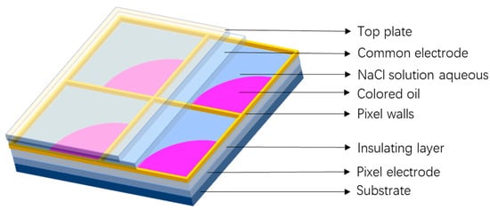 Figure 1 14 pages, 3392 KiB Open AccessArticle Green Anisole as Antisolvent in Planar Triple-Cation Perovskite Solar Cells with Varying Cesium Concentrations byVera La Ferrara, Antonella De Maria and Gabriella Rametta
Micromachines 2024, 15(1), 136; https://doi.org/10.3390/mi15010136 - 15 Jan 2024
Abstract
The feasibility of replacing toxic chlorobenzene antisolvents with environmentally friendly anisole in the fabrication of planar triple-cation perovskite solar cells was explored here. The successful integration of anisole not only ensures comparable device performance but also contributes to the development of more sustainable
[...] Read more.
The feasibility of replacing toxic chlorobenzene antisolvents with environmentally friendly anisole in the fabrication of planar triple-cation perovskite solar cells was explored here. The successful integration of anisole not only ensures comparable device performance but also contributes to the development of more sustainable and green fabrication processes for next-generation photovoltaic technologies. Nevertheless, to ensure the possibility of achieving well-functioning unencapsulated devices whose working operation depends on outdoor atmospheric conditions, we found that adjusting the cesium concentrations in the perovskite layers enabled the electrical characterization of efficient devices even under high relative humidity conditions (more than 40%). We found that 10% of CsI in the precursor solution will make devices with low hysteresis indexes and sustained performance stability over a 90-day period both with cholorobenzene and anisole antisolvent. These results further confirm that green anisole can replace chlorobenzene as an antisolvent.
Full article
(This article belongs to the Special Issue Nanostructures for Application in Electronics and Renewable Energy Sources)
►▼
Show Figures
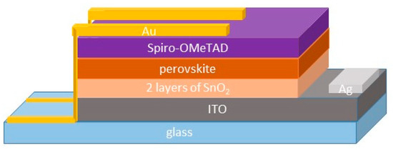 Figure 1 11 pages, 2691 KiB Open AccessArticle Ultra-High Frequency Surface Acoustic Wave Sensors for Temperature Detection byQi Dong, Qutong Yang, Xiaoyang Liu, Shenghe Hu, Wenzhe Nie, Zhao Jiang, Xiaoming Fan, Jingting Luo, Ran Tao and Chen Fu
Micromachines 2024, 15(1), 135; https://doi.org/10.3390/mi15010135 - 15 Jan 2024
Abstract
Highly sensitive surface acoustic wave (SAW) sensors have recently been recognized as a promising tool for various industrial and medical applications. However, existing SAW sensors generally suffer from a complex design, large size, and poor robustness. In this paper, we develop a simple
[...] Read more.
Highly sensitive surface acoustic wave (SAW) sensors have recently been recognized as a promising tool for various industrial and medical applications. However, existing SAW sensors generally suffer from a complex design, large size, and poor robustness. In this paper, we develop a simple and stable delay line ultra-high frequency (UHF) SAW sensor for highly sensitive detection of temperature. A Z-shaped delay line is specially designed on the piezoelectric substrate to improve the sensitivity and reduce the substrate size. Herein, the optimum design parameters of extremely short-pitch interdigital transducers (IDTs) are given by numerical simulations. The extremely short pitch gives the SAW sensor ultra-high operating frequency and consequently ultra-high sensitivity. Several experiments are conducted to demonstrate that the sensitivity of the Z-shaped SAW delay line sensor can reach up to 116.685°/°C for temperature detection. The results show that the sensor is an attractive alternative to current SAW sensing platforms in many applications.
Full article
(This article belongs to the Special Issue Novel Surface and Bulk Acoustic Wave Devices)
►▼
Show Figures
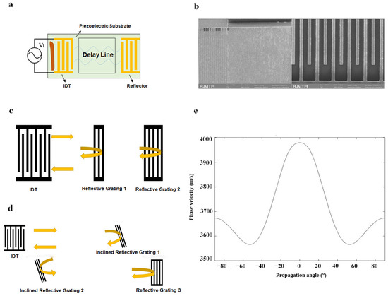 Figure 1 17 pages, 6309 KiB Open AccessArticle Modeling for High-Frequency Spurious Responses in Incredible High-Performance Surface Acoustic Wave Devices byGuanzhen Jiang, Yao Shuai, Zijie Wei, Jialin Yao, Wenbo Luo, Xinqiang Pan, Chuangui Wu and Wanli Zhang
Micromachines 2024, 15(1), 134; https://doi.org/10.3390/mi15010134 - 15 Jan 2024
Abstract
To ensure that surface acoustic wave (SAW) filters fulfill the requirements of Carrier Aggregation (CA) applications, the development of modeling tools that can forecast and simulate high-frequency spurious responses has been necessary. This paper presents an advanced methodology for extending the coupling-of-modes (COM)
[...] Read more.
To ensure that surface acoustic wave (SAW) filters fulfill the requirements of Carrier Aggregation (CA) applications, the development of modeling tools that can forecast and simulate high-frequency spurious responses has been necessary. This paper presents an advanced methodology for extending the coupling-of-modes (COM) model to obtain precise modeling of the high-frequency spurious responses of incredible high-performance surface acoustic wave (I.H.P. SAW) devices. The extended COM (ECOM) model is derived by modifying the conventional COM model and extending it accordingly. The parameters used in this model are determined through numerical fitting. For validation, firstly, the ECOM model is applied to a one-port synchronous I.H.P. SAW resonator, and the simulation and measurement results match. Then, the structural parameters of the ECOM model are varied, and the accuracy of the model after the structural parameters are varied is verified. It is demonstrated that this model can be applied to the design work of SAW filters. Finally, the ECOM model is applied to the design of the I.H.P. SAW filter based on a 42°YX-LiTaO3 (LT)/SiO2/AlN/Si structure. By using this method, the I.H.P. SAW filter’s high-frequency spurious response can be predicted more accurately.
Full article
►▼
Show Figures
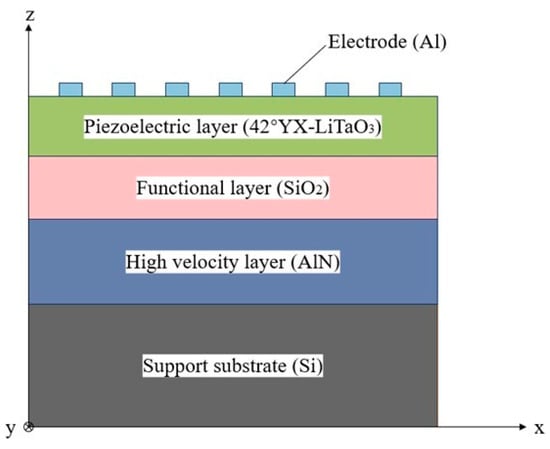 Figure 1 10 pages, 4841 KiB Open AccessArticle A 2.8 kV Breakdown Voltage α-Ga2O3 MOSFET with Hybrid Schottky Drain Contact bySeung Yoon Oh, Yeong Je Jeong, Inho Kang, Ji-Hyeon Park, Min Jae Yeom, Dae-Woo Jeon and Geonwook Yoo
Micromachines 2024, 15(1), 133; https://doi.org/10.3390/mi15010133 - 14 Jan 2024
Abstract
Among various polymorphic phases of gallium oxide (Ga2O3), α-phase Ga2O3 has clear advantages such as its heteroepitaxial growth as well as wide bandgap, which is promising for use in power devices. In this work, we demonstrate
[...] Read more.
Among various polymorphic phases of gallium oxide (Ga2O3), α-phase Ga2O3 has clear advantages such as its heteroepitaxial growth as well as wide bandgap, which is promising for use in power devices. In this work, we demonstrate α-Ga2O3 MOSFETs with hybrid Schottky drain (HSD) contact, comprising both Ohmic and Schottky electrode regions. In comparison with conventional Ohmic drain (OD) contact, a lower on-resistance (Ron) of 2.1 kΩ mm is achieved for variable channel lengths. Physics-based TCAD simulation is performed to validate the turn-on characteristics of the Schottky electrode region and the improved Ron. Electric-field analysis in the off-state is conducted for both the OD and HSD devices. Furthermore, a record breakdown voltage (BV) of 2.8 kV is achieved, which is superior to the 1.7 kV of the compared OD device. Our results show that the proposed HSD contact with a further optimized design can be a promising drain electrode scheme for α-Ga2O3 power MOSFETs.
Full article
(This article belongs to the Special Issue Power Semiconductor Devices and Applications, 2nd Edition)
►▼
Show Figures
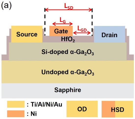 Figure 1 attachment Supplementary material: Supplementary File 1 (ZIP, 40756 KiB) 19 pages, 9320 KiB Open AccessArticle Low Profile Triangle-Shaped Piezoelectric Rotary Motor byAndrius Čeponis, Vytautas Jūrėnas and Dalius Mažeika
Micromachines 2024, 15(1), 132; https://doi.org/10.3390/mi15010132 - 13 Jan 2024
Abstract
In this paper, we present research on a novel low-profile piezoelectric rotary motor with a triangle-shaped stator. The stator of the motor comprises three interconnected piezoelectric bimorph plates forming an equilateral triangle. Bimorph plates consist of a passive layer fabricated from stainless steel
[...] Read more.
In this paper, we present research on a novel low-profile piezoelectric rotary motor with a triangle-shaped stator. The stator of the motor comprises three interconnected piezoelectric bimorph plates forming an equilateral triangle. Bimorph plates consist of a passive layer fabricated from stainless steel and four piezo ceramic plates glued to the upper and lower surfaces. Furthermore, spherical contacts are positioned on each bimorph plate at an offset from the plate’s center. Vibrations from the stator are induced by a single sawtooth-type electric signal while the frequency of the excitation signal is close to the resonant frequency of the second out-of-plane bending mode of the bimorph plate. The offset of the spherical contacts allows for a half-elliptical motion trajectory. By contrast, the forward and backward motion velocities of the contacts differ due to the asymmetrical excitation signal. The inertial principle of the motor and the angular motion of the rotor were obtained. Numerical and experimental investigations showed that the motor operates at a frequency of 21.18 kHz and achieves a maximum angular speed of 118 RPM at a voltage of 200 Vp-p. Additionally, an output torque of 18.3 mN·mm was obtained under the same voltage. The ratio between motor torque and weight is 36 mN·mm/g, while the ratio of angular speed and weight is 28.09 RPM/g.
Full article
(This article belongs to the Special Issue Recent Advance in Piezoelectric Actuators and Motors 2023)
►▼
Show Figures
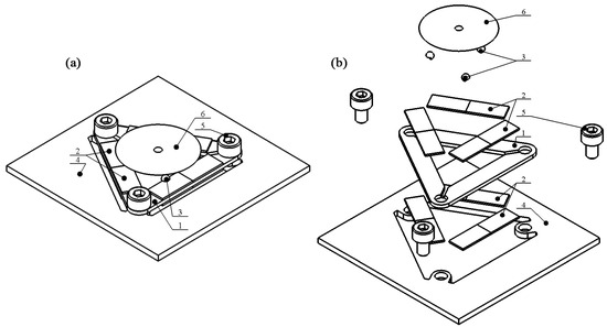 Figure 1 attachment Supplementary material: Supplementary File 1 (ZIP, 32301 KiB) 21 pages, 11892 KiB Open AccessArticle Scaling a Hydraulic Motor for Minimally Invasive Medical Devices byManjeera Vinnakota,  Kishan Bellur, Sandra L. Starnes and Mark J. Schulz
Micromachines 2024, 15(1), 131; https://doi.org/10.3390/mi15010131 - 12 Jan 2024
Abstract
Aligned with the medical device industry’s trend of miniaturization, academic and commercial researchers are constantly attempting to reduce device sizes. Many applications require miniature actuators (2 mm range) to perform mechanical work; however, biocompatible micromotors are not readily available. To that end, a
[...] Read more.
Aligned with the medical device industry’s trend of miniaturization, academic and commercial researchers are constantly attempting to reduce device sizes. Many applications require miniature actuators (2 mm range) to perform mechanical work; however, biocompatible micromotors are not readily available. To that end, a hydraulic motor-driven cutting module that aims to combine cutting and drug delivery is presented. The hydraulic motor prototype developed has an outside diameter (OD) of ~4 mm (twice the target size) and a 1 mm drive shaft to attach a cutter. Four different designs were explored and fabricated using additive manufacturing. The benchtop experimental data of the prototypes are presented herein. For the prototype motor with fluid inlet perpendicular to the blades, the average angular velocity was 10,593 RPM at a flowrate of 3.6 mL/s and 42,597 RPM at 10.1 mL/s. This design was numerically modeled using 3D-transient simulations in ANSYS CFX (version 2022 R2) to determine the performance characteristics and the internal resistance of the motor. Simplified mathematical models were also used to compute and compare the peak torque with the simulation estimates. The viability of current design represents a crucial milestone in scaling the hydraulic motor to a 2 mm OD to power a microcutter.
Full article
(This article belongs to the Special Issue Micromachines Research and Development in North America)
►▼
Show Figures Kishan Bellur, Sandra L. Starnes and Mark J. Schulz
Micromachines 2024, 15(1), 131; https://doi.org/10.3390/mi15010131 - 12 Jan 2024
Abstract
Aligned with the medical device industry’s trend of miniaturization, academic and commercial researchers are constantly attempting to reduce device sizes. Many applications require miniature actuators (2 mm range) to perform mechanical work; however, biocompatible micromotors are not readily available. To that end, a
[...] Read more.
Aligned with the medical device industry’s trend of miniaturization, academic and commercial researchers are constantly attempting to reduce device sizes. Many applications require miniature actuators (2 mm range) to perform mechanical work; however, biocompatible micromotors are not readily available. To that end, a hydraulic motor-driven cutting module that aims to combine cutting and drug delivery is presented. The hydraulic motor prototype developed has an outside diameter (OD) of ~4 mm (twice the target size) and a 1 mm drive shaft to attach a cutter. Four different designs were explored and fabricated using additive manufacturing. The benchtop experimental data of the prototypes are presented herein. For the prototype motor with fluid inlet perpendicular to the blades, the average angular velocity was 10,593 RPM at a flowrate of 3.6 mL/s and 42,597 RPM at 10.1 mL/s. This design was numerically modeled using 3D-transient simulations in ANSYS CFX (version 2022 R2) to determine the performance characteristics and the internal resistance of the motor. Simplified mathematical models were also used to compute and compare the peak torque with the simulation estimates. The viability of current design represents a crucial milestone in scaling the hydraulic motor to a 2 mm OD to power a microcutter.
Full article
(This article belongs to the Special Issue Micromachines Research and Development in North America)
►▼
Show Figures
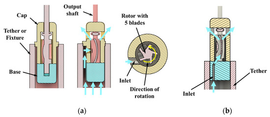 Figure 1 15 pages, 6933 KiB Open AccessArticle Development of a Microheater with a Large Heating Area and Low Thermal Stress in the Heating Area byTao Zhang, Zequan Pan, Chunhua Zhang, Liuguang Xiong, Chunmei Yang, Jian Zhang, Mengjiao Shi, Yuhang Wang and Wen Qu
Micromachines 2024, 15(1), 130; https://doi.org/10.3390/mi15010130 - 12 Jan 2024
Abstract
In this paper, a microheater that can absorb thermal stress and has a large heating area is demonstrated by optimizing the structure and process of the microheater. Four symmetrically distributed elongated support beam structures were machined around the microheater via deep silicon etching.
[...] Read more.
In this paper, a microheater that can absorb thermal stress and has a large heating area is demonstrated by optimizing the structure and process of the microheater. Four symmetrically distributed elongated support beam structures were machined around the microheater via deep silicon etching. This design efficiently mitigates the deformation of the heated region caused by thermal expansion and enhances the structural stability of the microheater. The updated microheater no longer converts the work area into a thin film; instead, it creates a stable heating platform that can uniformly heat a work area measuring 10 × 10 mm2. The microheater is verified to have high temperature uniformity and structural stability in finite element simulation. Finally, thorough investigations of electrical–thermal–structural characterization were conducted. The test findings show that the new microheater can achieve 350 °C with a power consumption of 6 W and a thermal reaction time of 22 s. A scan of its whole plane reveals that the surface of the working area of the new microheater is flat and does not distort in response to variations in temperature, offering good structural stability.
Full article
(This article belongs to the Special Issue Micro- and Nano-Systems for Manipulation, Actuation and Sensing, 2nd Edition)
►▼
Show Figures
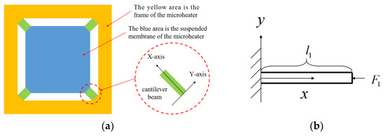 Figure 1 15 pages, 2244 KiB Open AccessArticle Accelerated Computational Fluid Dynamics Simulations of Microfluidic Devices by Exploiting Higher Levels of Abstraction byMichel Takken and Robert Wille
Micromachines 2024, 15(1), 129; https://doi.org/10.3390/mi15010129 - 12 Jan 2024
Abstract
The design of microfluidic devices is a cumbersome and tedious process that can be significantly improved by simulation. Methods based on Computational Fluid Dynamics (CFD) are considered state-of-the-art, but require extensive compute time—oftentimes limiting the size of microfluidic devices that can be simulated.
[...] Read more.
The design of microfluidic devices is a cumbersome and tedious process that can be significantly improved by simulation. Methods based on Computational Fluid Dynamics (CFD) are considered state-of-the-art, but require extensive compute time—oftentimes limiting the size of microfluidic devices that can be simulated. Simulation methods that abstract the underlying physics on a higher level generally provide results instantly, but the fidelity of these methods is usually worse. In this work, a simulation method that accelerates CFD simulations by exploiting simulation methods on higher levels of abstraction is proposed. Case studies confirm that the proposed method accelerates CFD simulations by multiple factors (often several orders of magnitude) while maintaining the fidelity of CFD simulations.
Full article
(This article belongs to the Special Issue Computational Tools and AI in Design and Micro-Manufacturing)
►▼
Show Figures
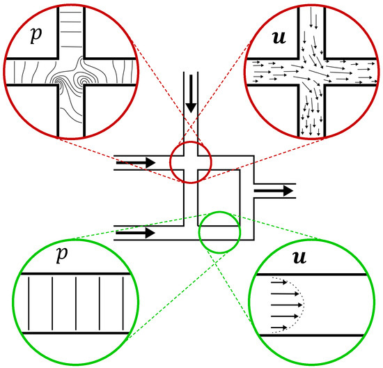 Figure 1 15 pages, 22815 KiB Open AccessArticle Lightweight and High-Stiffness Metal Optical Systems Based on Additive Manufacturing byQiang Fu, Lei Yan, Shuanglong Tan, Yang Liu and Lingjie Wang
Micromachines 2024, 15(1), 128; https://doi.org/10.3390/mi15010128 - 12 Jan 2024
Abstract
To build a long-wave infrared catadioptric optical system for deep space low-temperature target detection with a lightweight and wide field of view, this work conducted a study that encompasses a local cooling optical system, topology optimization-based metal mirror design, and additive manufacturing. First,
[...] Read more.
To build a long-wave infrared catadioptric optical system for deep space low-temperature target detection with a lightweight and wide field of view, this work conducted a study that encompasses a local cooling optical system, topology optimization-based metal mirror design, and additive manufacturing. First, a compact catadioptric optical system with local cooling was designed. This system features a 55 mm aperture, a 110 mm focal length, and a 4-degree by 4-degree field of view. Secondly, we applied the principles of topology optimization to design the primary mirror assembly, the secondary mirror assembly, and the connecting baffle. The third and fourth modes achieved a resonance frequency of 1213.7 Hz. Then, we manufactured the mirror assemblies using additive manufacturing and single-point diamond turning, followed by the centering assembly method to complete the optical assembly. Lastly, we conducted performance testing on the system, with the test results revealing that the modulation transfer function (MTF) curves of the optical system reached the diffraction limit across the entire field of view. Remarkably, the system’s weight was reduced to a mere 96.04 g. The use of additive manufacturing proves to be an effective means of enhancing optical system performance.
Full article
(This article belongs to the Special Issue 3D Printing Technology and Its Applications)
►▼
Show Figures
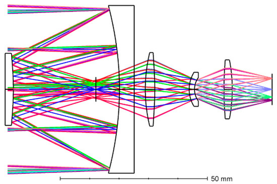 Figure 1 More Articles... More News & Announcements...
Topics
Propose a Topic
Topic in
Applied Sciences, Computers, Electronics, Micromachines, Sustainability
Innovation of Applied System
Topic Editors: Sheng-Joue Young, Shoou-Jinn Chang, Liang-Wen JiDeadline: 31 January 2024
Topic in
Applied Sciences, Fibers, Micromachines, Molecules, Photonics
Recent Advances in Nonlinear Optics and Nonlinear Optical Materials
Topic Editors: You Wang, Jiyong Yao, Zheng Xie, Yan FengDeadline: 1 April 2024
Topic in
Bioengineering, JMMP, Materials, Micromachines, Polymers
Advances in Filament Engineering for Biomaterials
Topic Editors: Ming-Wei Chang, Zeeshan Ahmad, Hui-Min David WangDeadline: 30 June 2024
Topic in
Chemistry, Materials, Micromachines, Molecules, Photonics
Materials, Structure Designs and Device Fabrications for Highly Efficient/Long Lifetime Organic Light-Emitting Diodes
Topic Editors: Ping Chen, Jwo-Huei JouDeadline: 31 December 2024
More Topics
More News & Announcements...
Topics
Propose a Topic
Topic in
Applied Sciences, Computers, Electronics, Micromachines, Sustainability
Innovation of Applied System
Topic Editors: Sheng-Joue Young, Shoou-Jinn Chang, Liang-Wen JiDeadline: 31 January 2024
Topic in
Applied Sciences, Fibers, Micromachines, Molecules, Photonics
Recent Advances in Nonlinear Optics and Nonlinear Optical Materials
Topic Editors: You Wang, Jiyong Yao, Zheng Xie, Yan FengDeadline: 1 April 2024
Topic in
Bioengineering, JMMP, Materials, Micromachines, Polymers
Advances in Filament Engineering for Biomaterials
Topic Editors: Ming-Wei Chang, Zeeshan Ahmad, Hui-Min David WangDeadline: 30 June 2024
Topic in
Chemistry, Materials, Micromachines, Molecules, Photonics
Materials, Structure Designs and Device Fabrications for Highly Efficient/Long Lifetime Organic Light-Emitting Diodes
Topic Editors: Ping Chen, Jwo-Huei JouDeadline: 31 December 2024
More Topics
 Conferences
Announce Your Conference
1–4 August 2024
The 1st International Conference on AI Sensors and The 10th International Symposium on Sensor Science
Conferences
Announce Your Conference
1–4 August 2024
The 1st International Conference on AI Sensors and The 10th International Symposium on Sensor Science 21–23 February 2024
The 5th International Conference on Microfluidic Handling Systems
21–23 February 2024
The 5th International Conference on Microfluidic Handling Systems 26–28 February 2024
5th International Conference on Materials Science, Engineering & Technology
26–28 February 2024
5th International Conference on Materials Science, Engineering & Technology More Conferences...
Special Issues
Propose a Special Issue
Special Issue in
Micromachines
Quantum Photonics: Development and Applications
Guest Editor: Gonzalo CarvachoDeadline: 20 January 2024
Special Issue in
Micromachines
SiC Applications outside Power Electronic Devices
Guest Editors: Alberto Roncaglia, Francesco La ViaDeadline: 31 January 2024
Special Issue in
Micromachines
Piezoelectric MEMS/NEMS—Materials, Devices, and Applications, Volume II
Guest Editor: Wei LiDeadline: 15 February 2024
Special Issue in
Micromachines
MEMS Sensors: Past, Present and Future
Guest Editors: Liangcheng Tu, Wenjie WuDeadline: 28 February 2024
More Special Issues
Topical Collections
Topical Collection in
Micromachines
Micromixers: Analysis, Design and Fabrication
Collection Editor: Kwang-Yong Kim
Topical Collection in
Micromachines
Lab-on-a-Chip
Collection Editors: Jeong-Bong Lee, Ning Xue
Topical Collection in
Micromachines
Piezoelectric Transducers: Materials, Devices and Applications
Collection Editor: Jose Luis Sanchez-Rojas
Topical Collection in
Micromachines
Women in Micromachines
Collection Editors: Anna Vikulina, Regina Luttge
More Topical Collections
Micromachines,
EISSN 2072-666X,
Published by MDPI
RSS
Content Alert
Further Information
Article Processing Charges
Pay an Invoice
Open Access Policy
Contact MDPI
Jobs at MDPI
Guidelines
For Authors
For Reviewers
For Editors
For Librarians
For Publishers
For Societies
For Conference Organizers
MDPI Initiatives
Sciforum
MDPI Books
Preprints.org
Scilit
SciProfiles
Encyclopedia
JAMS
Proceedings Series
Follow MDPI
LinkedIn
Facebook
Twitter
More Conferences...
Special Issues
Propose a Special Issue
Special Issue in
Micromachines
Quantum Photonics: Development and Applications
Guest Editor: Gonzalo CarvachoDeadline: 20 January 2024
Special Issue in
Micromachines
SiC Applications outside Power Electronic Devices
Guest Editors: Alberto Roncaglia, Francesco La ViaDeadline: 31 January 2024
Special Issue in
Micromachines
Piezoelectric MEMS/NEMS—Materials, Devices, and Applications, Volume II
Guest Editor: Wei LiDeadline: 15 February 2024
Special Issue in
Micromachines
MEMS Sensors: Past, Present and Future
Guest Editors: Liangcheng Tu, Wenjie WuDeadline: 28 February 2024
More Special Issues
Topical Collections
Topical Collection in
Micromachines
Micromixers: Analysis, Design and Fabrication
Collection Editor: Kwang-Yong Kim
Topical Collection in
Micromachines
Lab-on-a-Chip
Collection Editors: Jeong-Bong Lee, Ning Xue
Topical Collection in
Micromachines
Piezoelectric Transducers: Materials, Devices and Applications
Collection Editor: Jose Luis Sanchez-Rojas
Topical Collection in
Micromachines
Women in Micromachines
Collection Editors: Anna Vikulina, Regina Luttge
More Topical Collections
Micromachines,
EISSN 2072-666X,
Published by MDPI
RSS
Content Alert
Further Information
Article Processing Charges
Pay an Invoice
Open Access Policy
Contact MDPI
Jobs at MDPI
Guidelines
For Authors
For Reviewers
For Editors
For Librarians
For Publishers
For Societies
For Conference Organizers
MDPI Initiatives
Sciforum
MDPI Books
Preprints.org
Scilit
SciProfiles
Encyclopedia
JAMS
Proceedings Series
Follow MDPI
LinkedIn
Facebook
Twitter
|
【本文地址】